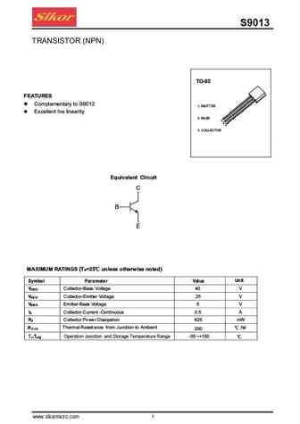
9013G Datasheet. Specs and Replacement
Type Designator: 9013G 📄📄
Material of Transistor: Si
Polarity: NPN
Absolute Maximum Ratings
Maximum Collector Power Dissipation (Pc): 0.4 W
Maximum Collector-Base Voltage |Vcb|: 25 V
Maximum Collector-Emitter Voltage |Vce|: 25 V
Maximum Emitter-Base Voltage |Veb|: 3 V
Maximum Collector Current |Ic max|: 0.4 A
Max. Operating Junction Temperature (Tj): 150 °C
Electrical Characteristics
Transition Frequency (ft): 50 MHz
Collector Capacitance (Cc): 3.5 pF
Forward Current Transfer Ratio (hFE), MIN: 118
Package: TO92
📄📄 Copy
9013G Substitution
- BJT ⓘ Cross-Reference Search
9013G datasheet
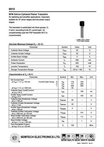
9013 NPN Silicon Epitaxial Planar Transistor for switching and amplifier applications. Especially suitable for AF-driver stages and low power output stages. The transistor is subdivided into three groups, G, H and I, according to its DC current gain. As complementary type the PNP transistor 9012 is recommended. 1. Emitter 2. Base 3. Collector TO-92 Plastic Package O Absol... See More ⇒
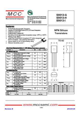
MCC S9013-G TM Micro Commercial Components 20736 Marilla Street Chatsworth S9013-H Micro Commercial Components CA 91311 S9013-I Phone (818) 701-4933 Fax (818) 701-4939 Features TO-92 Plastic-Encapsulate Transistors Capable of 0.625Watts(Tamb=25OC) of Power Dissipation. NPN Silicon Collector-current 0.5A Collector-base Voltage 40V Transistors Operating and... See More ⇒
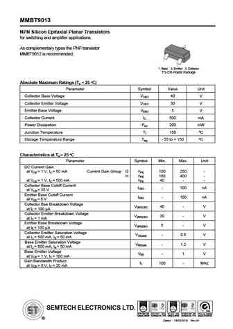
MMBT9013 NPN Silicon Epitaxial Planar Transistors for switching and amplifier applications. As complementary types the PNP transistor MMBT9012 is recommended. TO-236 Plastic Package O Absolute Maximum Ratings (Ta = 25 C) Parameter Symbol Value Unit Collector Base Voltage VCBO 40 V Collector Emitter Voltage VCEO 30 V Emitter Base Voltage VEBO 5 V Collector Current IC 500 mA Po... See More ⇒
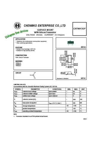
CHENMKO ENTERPRISE CO.,LTD CHT9013GP SURFACE MOUNT NPN Silicon Transistor VOLTAGE 25Volts CURRENT 0.5 Ampere APPLICATION * Telephony and proferssional communction equipment. * Other switching applications. SOT-23 FEATURE * Surface mount package. (SOT-23) * Suitable for high packing density. (1) CONSTRUCTION (3) *NPN Silicon Transistor (2) MARKING * HFE(L) J3 ( ) ( ) .055 1.... See More ⇒
Detailed specifications: 9012E, 9012F, 9012G, 9012H, 9013, 9013D, 9013E, 9013F, 2SA1837, 9013H, 9014, 9014D, 9014E, 9014F, 9014G, 9014H, 9015
Keywords - 9013G pdf specs
9013G cross reference
9013G equivalent finder
9013G pdf lookup
9013G substitution
9013G replacement
BJT Parameters and How They Relate
🌐 : EN ES РУ
LIST
Last Update
BJT: ZDT6705 | GA1L4Z | GA1A4M | SBT42 | 2SA200-Y | 2SA200-O
Popular searches
2sa750 datasheet | 2sa940 transistor datasheet | 2sb549 | 5n50 mosfet equivalent | a1016 transistor | a1693 transistor | a933 datasheet | c535 transistor
