2N1000 Datasheet. Specs and Replacement
Type Designator: 2N1000 📄📄
Material of Transistor: Ge
Polarity: NPN
Absolute Maximum Ratings
Maximum Collector Power Dissipation (Pc): 0.15 W
Maximum Collector-Base Voltage |Vcb|: 25 V
Maximum Collector-Emitter Voltage |Vce|: 25 V
Maximum Emitter-Base Voltage |Veb|: 40 V
Max. Operating Junction Temperature (Tj): 100 °C
Electrical Characteristics
Transition Frequency (ft): 6 MHz
Collector Capacitance (Cc): 20 pF
Forward Current Transfer Ratio (hFE), MIN: 40
Noise Figure, dB: -
Package: TO5
📄📄 Copy
- BJT ⓘ Cross-Reference Search
2N1000 datasheet
9.1. Size:731K fairchild semi
fqd2n100tf fqd2n100tm fqd2n100 fqu2n100 fqu2n100tu.pdf 

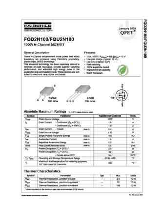
January 2009 QFET FQD2N100/FQU2N100 1000V N-Channel MOSFET General Description Features These N-Channel enhancement mode power field effect 1.6A, 1000V, RDS(on) = 9 @VGS = 10 V transistors are produced using Fairchild s proprietary, Low gate charge ( typical 12 nC) planar stripe, DMOS technology. Low Crss ( typical 5 pF) This advanced technology has been especially t... See More ⇒
9.2. Size:50K ixys
ixgp12n100.pdf 

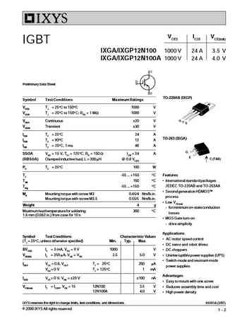
VCES IC25 VCE(sat) IGBT IXGA/IXGP12N100 1000 V 24 A 3.5 V IXGA/IXGP12N100A 1000 V 24 A 4.0 V Preliminary Data Sheet TO-220AB (IXGP) Symbol Test Conditions Maximum Ratings VCES TJ = 25 C to 150 C 1000 V VCGR TJ = 25 C to 150 C; RGE = 1 MW 1000 V G VGES Continuous 20 V C E VGEM Transient 30 V IC25 TC = 25 C24 A TO-263 (IXGA) IC90 TC = 90 C12 A ICM TC = 25 C, 1 ms 48 A ... See More ⇒
9.3. Size:105K ixys
ixth10n100 ixtm10n100 ixth12n100 ixtm12n100.pdf 

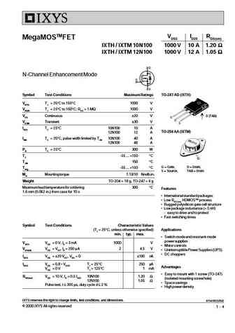
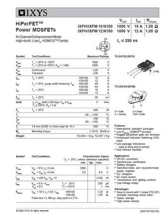
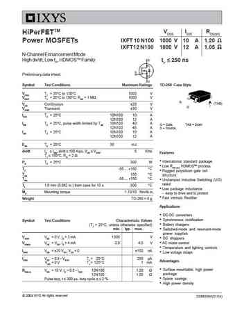
VDSS ID25 RDS(on) MegaMOSTMFET IXTH / IXTM 10N100 1000 V 10 A 1.20 IXTH / IXTM 12N100 1000 V 12 A 1.05 N-Channel Enhancement Mode Symbol Test Conditions Maximum Ratings TO-247 AD (IXTH) VDSS TJ = 25 C to 150 C 1000 V VDGR TJ = 25 C to 150 C; RGS = 1 M 1000 V VGS Continuous 20 V D (TAB) VGSM Transient 30 V ID25 TC = 25 C 10N... See More ⇒
9.4. Size:119K ixys
ixgh12n100u1.pdf 

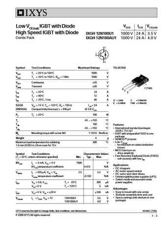
VCES IC25 VCE(sat) Low VCE(sat) IGBT with Diode High Speed IGBT with Diode IXGH 12N100U1 1000 V 24 A 3.5 V Combi Pack IXGH 12N100AU1 1000 V 24 A 4.0 V Symbol Test Conditions Maximum Ratings TO-247AD VCES TJ = 25 C to 150 C 1000 V VCGR TJ = 25 C to 150 C; RGE = 1 MW 1000 V VGES Continuous 20 V VGEM Transient 30 V C (TAB) G C IC25 TC = 25 C24 A E IC90 TC = 90 C12 A ICM ... See More ⇒
9.6. Size:83K ixys
ixgp2n100a.pdf 

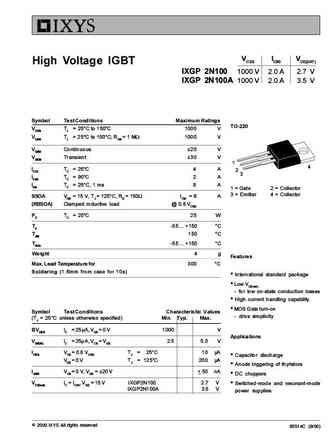
VCES IC90 VCE(SAT) High Voltage IGBT IXGP 2N100 1000 V 2.0 A 2.7 V IXGP 2N100A 1000 V 2.0 A 3.5 V Symbol Test Conditions Maximum Ratings TO-220 VCES TJ = 25 C to 150 C 1000 V VCGR TJ = 25 C to 150 C; RGE = 1 MW 1000 V VGES Continuous 20 V VGEM Transient 30 V 1 4 IC25 TC = 25 C 4 A 2 3 IC90 TC = 90 C 2 A ICM TC = 25 C, 1 ms 8 A 1 = Gate 2 = Collector 3 = Emitter 4 = ... See More ⇒
9.7. Size:50K ixys
ixgp12n100a.pdf 

VCES IC25 VCE(sat) IGBT IXGA/IXGP12N100 1000 V 24 A 3.5 V IXGA/IXGP12N100A 1000 V 24 A 4.0 V Preliminary Data Sheet TO-220AB (IXGP) Symbol Test Conditions Maximum Ratings VCES TJ = 25 C to 150 C 1000 V VCGR TJ = 25 C to 150 C; RGE = 1 MW 1000 V G VGES Continuous 20 V C E VGEM Transient 30 V IC25 TC = 25 C24 A TO-263 (IXGA) IC90 TC = 90 C12 A ICM TC = 25 C, 1 ms 48 A ... See More ⇒
9.8. Size:119K ixys
ixgh12n100au1.pdf 

VCES IC25 VCE(sat) Low VCE(sat) IGBT with Diode High Speed IGBT with Diode IXGH 12N100U1 1000 V 24 A 3.5 V Combi Pack IXGH 12N100AU1 1000 V 24 A 4.0 V Symbol Test Conditions Maximum Ratings TO-247AD VCES TJ = 25 C to 150 C 1000 V VCGR TJ = 25 C to 150 C; RGE = 1 MW 1000 V VGES Continuous 20 V VGEM Transient 30 V C (TAB) G C IC25 TC = 25 C24 A E IC90 TC = 90 C12 A ICM ... See More ⇒
9.9. Size:84K ixys
ixgp12n100u1.pdf 

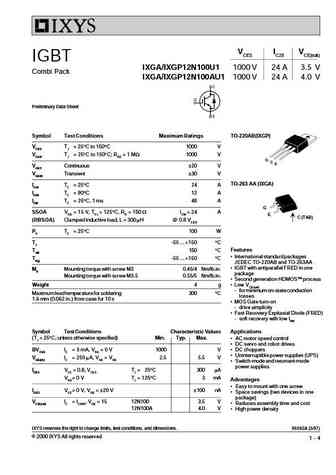
VCES IC25 VCE(sat) IGBT IXGA/IXGP12N100U1 1000 V 24 A 3.5 V Combi Pack IXGA/IXGP12N100AU1 1000 V 24 A 4.0 V Preliminary Data Sheet Symbol Test Conditions Maximum Ratings TO-220AB(IXGP) VCES TJ = 25 C to 150 C 1000 V VCGR TJ = 25 C to 150 C; RGE = 1 MW 1000 V G C E VGES Continuous 20 V VGEM Transient 30 V TO-263 AA (IXGA) IC25 TC = 25 C24 A IC90 TC = 90 C12 A ICM TC = ... See More ⇒
9.11. Size:34K ixys
ixgh12n100.pdf 

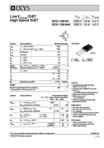
VCES IC25 VCE(sat) Low VCE(sat) IGBT High Speed IGBT IXGH 12N100 1000 V 24 A 3.5 V IXGH 12N100A 1000 V 24 A 4.0 V Symbol Test Conditions Maximum Ratings TO-247AD VCES TJ = 25 C to 150 C 1000 V VCGR TJ = 25 C to 150 C; RGE = 1 MW 1000 V VGES Continuous 20 V C (TAB) G C VGEM Transient 30 V E IC25 TC = 25 C24 A G = Gate C = Collector IC90 TC = 90 C12 A E = Emitter TAB = ... See More ⇒
9.12. Size:120K ixys
ixgt32n100a3.pdf 

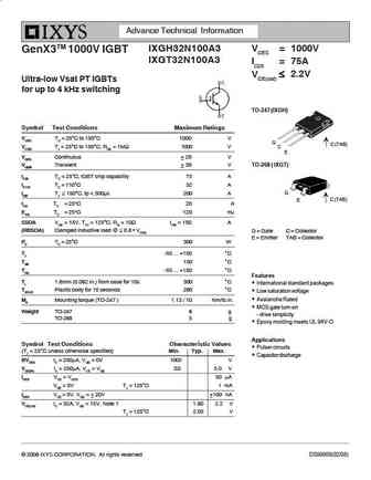
Advance Technical Information IXGH32N100A3 VCES = 1000V GenX3TM 1000V IGBT IXGT32N100A3 IC25 = 75A VCE(sat) 2.2V Ultra-low Vsat PT IGBTs for up to 4 kHz switching TO-247 (IXGH) Symbol Test Conditions Maximum Ratings VCES TC = 25 C to 150 C 1000 V G C (TAB) VCGR TJ = 25 C to 150 C, RGE = 1M 1000 V C E VGES Continuous 20 V TO-268 ( ... See More ⇒
9.13. Size:148K ixys
ixft12n100qhv.pdf 

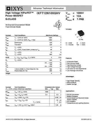
Advance Technical Information High Voltage HiPerFETTM VDSS = 1000V IXFT12N100QHV Power MOSFET ID25 = 12A Q-CLASS RDS(on) 1.05 N-Channel Enhancement Mode Fast Intrinsic Diode TO-268S G Symbol Test Conditions Maximum Ratings S VDSS TJ = 25 C to 150 C 1000 V D (Tab) VDGR TJ = 25 C to 150 C, RGS = 1M 1000 V VGSS Continuous 20 V G = Ga... See More ⇒
9.14. Size:83K ixys
ixgp2n100.pdf 

VCES IC90 VCE(SAT) High Voltage IGBT IXGP 2N100 1000 V 2.0 A 2.7 V IXGP 2N100A 1000 V 2.0 A 3.5 V Symbol Test Conditions Maximum Ratings TO-220 VCES TJ = 25 C to 150 C 1000 V VCGR TJ = 25 C to 150 C; RGE = 1 MW 1000 V VGES Continuous 20 V VGEM Transient 30 V 1 4 IC25 TC = 25 C 4 A 2 3 IC90 TC = 90 C 2 A ICM TC = 25 C, 1 ms 8 A 1 = Gate 2 = Collector 3 = Emitter 4 = ... See More ⇒
9.15. Size:51K ixys
ixga12n100 ixgp12n100 ixga12n100a ixgp12n100a.pdf 

VCES IC25 VCE(sat) IGBT IXGA/IXGP12N100 1000 V 24 A 3.5 V IXGA/IXGP12N100A 1000 V 24 A 4.0 V Preliminary Data Sheet TO-220AB (IXGP) Symbol Test Conditions Maximum Ratings VCES TJ = 25 C to 150 C 1000 V VCGR TJ = 25 C to 150 C; RGE = 1 MW 1000 V G VGES Continuous 20 V C E VGEM Transient 30 V IC25 TC = 25 C24 A TO-263 (IXGA) IC90 TC = 90 C12 A ICM TC = 25 C, 1 ms 48 A ... See More ⇒
9.16. Size:116K ixys
ixga12n100u1 ixgp12n100u1 ixga12n100au1 ixgp12n100au1.pdf 

VCES IC25 VCE(sat) IGBT IXGA/IXGP12N100U1 1000 V 24 A 3.5 V Combi Pack IXGA/IXGP12N100AU1 1000 V 24 A 4.0 V Preliminary Data Sheet Symbol Test Conditions Maximum Ratings TO-220AB(IXGP) VCES TJ = 25 C to 150 C 1000 V VCGR TJ = 25 C to 150 C; RGE = 1 MW 1000 V G C E VGES Continuous 20 V VGEM Transient 30 V TO-263 AA (IXGA) IC25 TC = 25 C24 A IC90 TC = 90 C12 A ICM TC = ... See More ⇒
9.17. Size:120K ixys
ixgh32n100a3.pdf 

Advance Technical Information IXGH32N100A3 VCES = 1000V GenX3TM 1000V IGBT IXGT32N100A3 IC25 = 75A VCE(sat) 2.2V Ultra-low Vsat PT IGBTs for up to 4 kHz switching TO-247 (IXGH) Symbol Test Conditions Maximum Ratings VCES TC = 25 C to 150 C 1000 V G C (TAB) VCGR TJ = 25 C to 150 C, RGE = 1M 1000 V C E VGES Continuous 20 V TO-268 ( ... See More ⇒
9.18. Size:76K ixys
ixta2n100 ixtp2n100.pdf 

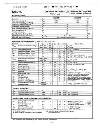
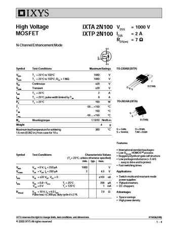
High Voltage VDSS = 1000 V IXTA 2N100 MOSFET ID25 = 2 A IXTP 2N100 RDS(on) = 7 N-Channel Enhancement Mode Symbol Test Conditions Maximum Ratings TO-220AB (IXTP) VDSS TJ = 25 C to 150 C 1000 V VDGR TJ = 25 C to 150 C; RGS = 1 M 1000 V VGS Continuous 20 V D (TAB) G VGSM Transient 30 V D S ID25 TC = 25 C2 A IDM TC = 25 C, pulse width limited by ... See More ⇒
9.19. Size:144K ixys
ixft12n100q ixfh12n100q ixft10n100q ixfh10n100q.pdf 

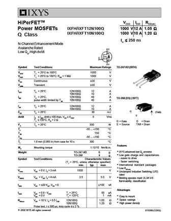
VDSS ID25 RDS(on) HiPerFETTM IXFH/IXFT12N100Q 1000 V 12 A 1.05 Power MOSFETs IXFH/IXFT10N100Q 1000 V 10 A 1.20 Q Class trr 250 ns N-Channel Enhancement Mode Avalanche Rated Low Qg, High dv/dt Symbol Test Conditions Maximum Ratings TO-247 AD (IXFH) VDSS TJ = 25 C to 150 C 1000 V VDGR TJ = 25 C to 150 C; RGS... See More ⇒
9.20. Size:34K ixys
ixgh12n100a.pdf 

VCES IC25 VCE(sat) Low VCE(sat) IGBT High Speed IGBT IXGH 12N100 1000 V 24 A 3.5 V IXGH 12N100A 1000 V 24 A 4.0 V Symbol Test Conditions Maximum Ratings TO-247AD VCES TJ = 25 C to 150 C 1000 V VCGR TJ = 25 C to 150 C; RGE = 1 MW 1000 V VGES Continuous 20 V C (TAB) G C VGEM Transient 30 V E IC25 TC = 25 C24 A G = Gate C = Collector IC90 TC = 90 C12 A E = Emitter TAB = ... See More ⇒
9.22. Size:97K ixys
ixfr10n100f ixfr12n100f.pdf 

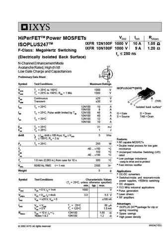
VDSS ID25 RDS(on) HiPerFETTM Power MOSFETs IXFR 12N100F 1000 V 10 A 1.05 ISOPLUS247TM IXFR 10N100F 1000 V 9 A 1.20 F-Class MegaHertz Switching trr 250 ns (Electrically Isolated Back Surface) N-Channel Enhancement Mode Avalanche Rated, High dV/dt Low Gate Charge and Capacitances Preliminary Data Sheet Symbol ... See More ⇒
9.23. Size:245K ixys
ixz4df12n100.pdf 

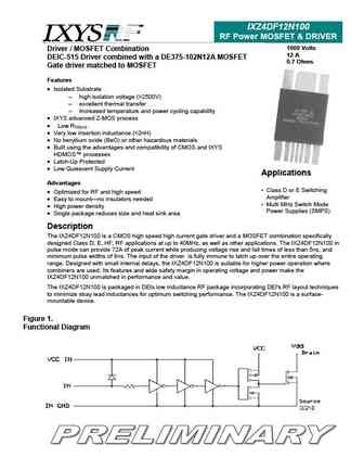
IXZ4DF12N100 RF Power MOSFET & DRIVER 1000 Volts Driver / MOSFET Combination 12 A DEIC-515 Driver combined with a DE375-102N12A MOSFET 0.7 Ohms Gate driver matched to MOSFET Features Isolated Substrate - high isolation voltage (>2500V) - excellent thermal transfer - Increased temperature and power cycling capability IXYS advanced Z-MOS process Low RDS(on)... See More ⇒
9.24. Size:84K ixys
ixgp12n100au1.pdf 

VCES IC25 VCE(sat) IGBT IXGA/IXGP12N100U1 1000 V 24 A 3.5 V Combi Pack IXGA/IXGP12N100AU1 1000 V 24 A 4.0 V Preliminary Data Sheet Symbol Test Conditions Maximum Ratings TO-220AB(IXGP) VCES TJ = 25 C to 150 C 1000 V VCGR TJ = 25 C to 150 C; RGE = 1 MW 1000 V G C E VGES Continuous 20 V VGEM Transient 30 V TO-263 AA (IXGA) IC25 TC = 25 C24 A IC90 TC = 90 C12 A ICM TC = ... See More ⇒
9.25. Size:33K ixys
ixfr10n100q ixfr12n100q.pdf 

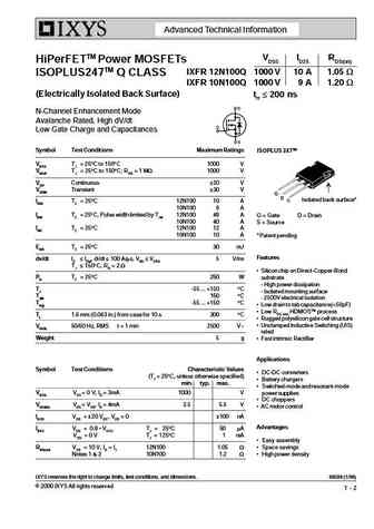
Advanced Technical Information VDSS ID25 RDS(on) HiPerFETTM Power MOSFETs IXFR 12N100Q 1000 V 10 A 1.05 W ISOPLUS247TM Q CLASS IXFR 10N100Q 1000 V 9 A 1.20 W (Electrically Isolated Back Surface) trr 200 ns N-Channel Enhancement Mode Avalanche Rated, High dV/dt Low Gate Charge and Capacitances Symbol Test Conditions Maximum Ratings ISOPLUS 247TM VDSS TJ = 25 C to 150 C 1000 V ... See More ⇒
9.26. Size:35K ixys
ixgh12n100 ixgh12n100a.pdf 

VCES IC25 VCE(sat) Low VCE(sat) IGBT High Speed IGBT IXGH 12N100 1000 V 24 A 3.5 V IXGH 12N100A 1000 V 24 A 4.0 V Symbol Test Conditions Maximum Ratings TO-247AD VCES TJ = 25 C to 150 C 1000 V VCGR TJ = 25 C to 150 C; RGE = 1 MW 1000 V VGES Continuous 20 V C (TAB) G C VGEM Transient 30 V E IC25 TC = 25 C24 A G = Gate C = Collector IC90 TC = 90 C12 A E = Emitter TAB = ... See More ⇒
9.27. Size:352K aosemi
aod2n100.pdf 

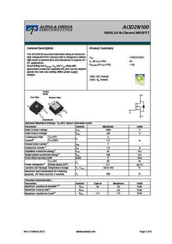
AOD2N100 1000V,2A N-Channel MOSFET General Description Product Summary The AOD2N100 has been fabricated using an advanced high voltage MOSFET process that is designed to deliver VDS 1100V@150 high levels of performance and robustness in popular AC- ID (at VGS=10V) 2A DC applications. RDS(ON) (at VGS=10V) ... See More ⇒
9.30. Size:4585K slkor
sl12n100t sl12n100k sl12n100 sl12n100f.pdf 

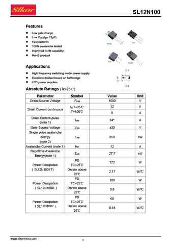
SL12N100 Features Low gate charge Low C (typ 13pF) rss Fast switchin 100% avalanche tested Improved dv/dt capability RoHS product Applications High frequency switching mode power supply Electronic ballast based on half bridge LED power supplies Absolute Ratings (Tc=25 ) Parameter Symbol Value Unit Drain-Source Voltage V 1000 V DSS 12 A I T... See More ⇒
9.31. Size:1190K way-on
wmo2n100d1 wmaa2n100d1.pdf 

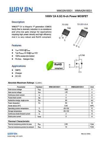
WMO2N100D1 WMAA2N100D1 1000V 2A 6.3 N-ch Power MOSFET Description TO-252 TO-251-L9.4 WMOSTM D1 is Wayon s 1st generation VDMOS TAB TAB family that is dramatic reduction in on-resistance and ultra-low gate charge for applications requiring high power density and high efficiency. And it is very robust and RoHS compliant. D G S G Features D S V =1050V... See More ⇒
9.32. Size:653K way-on
wml12n100c2 wmm12n100c2 wmn12n100c2 wmj12n100c2 wmk12n100c2.pdf 

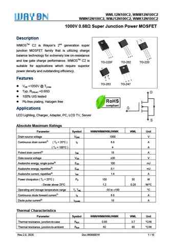
WML12N100C2, WMM C2 W M12N100C WMN12N WMJ12N10 K12N100C N100C2, W 00C2, WMK C2 1000V 0.68 S unction Power M T Super Ju MOSFET Descrip ption WMOSTM C2 is Wa 2nd generation super ayon s n junction MOSFET fa that is utilizing charge M amily S balance te or extremely esistance echnology fo y low on-re S D D G G G S D G and low ga charge performanc WMOSTM C... See More ⇒
9.33. Size:454K convert
cs2n100f cs2n100p cs2n100u cs2n100d.pdf 

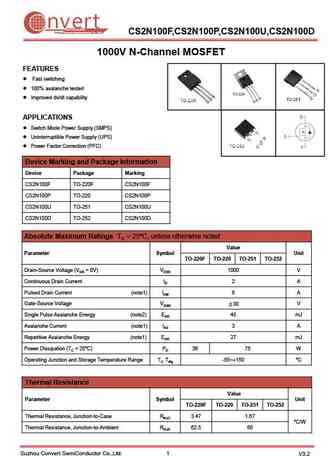
nvert Suzhou Convert Semiconductor Co ., Ltd. CS2N100F,CS2N100P,CS2N100U,CS2N100D 1000V N-Channel MOSFET FEATURES Fast switching 100% avalanche tested Improved dv/dt capability APPLICATIONS Switch Mode Power Supply (SMPS) Uninterruptible Power Supply (UPS) Power Factor Correction (PFC) Device Marking and Package Information Device Package Marking CS2N100F T... See More ⇒
9.34. Size:419K convert
cs2n100f cs2n100p cs2n100u.pdf 

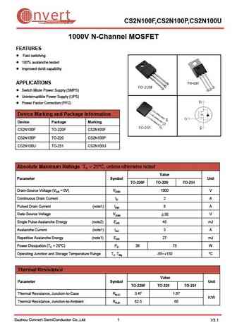
nvert CS2N100F,CS2N100P,CS2N100U Suzhou Convert Semiconductor Co ., Ltd. 1000V N-Channel MOSFET FEATURES Fast switching 100% avalanche tested Improved dv/dt capability APPLICATIONS Switch Mode Power Supply (SMPS) Uninterruptible Power Supply (UPS) Power Factor Correction (PFC) Device Marking and Package Information Device Package Marking CS2N100F TO-220F CS... See More ⇒
9.35. Size:395K convert
cs2n100lf.pdf 

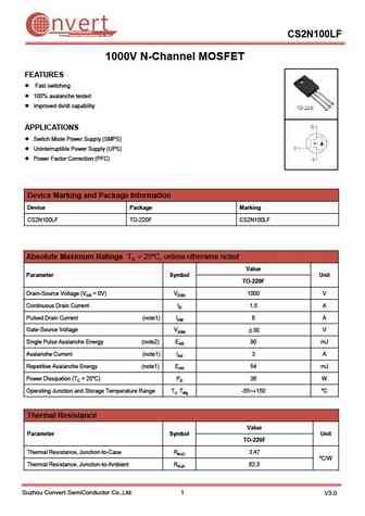
nvert Suzhou Convert Semiconductor Co ., Ltd. CS2N100LF 1000V N-Channel MOSFET FEATURES Fast switching 100% avalanche tested Improved dv/dt capability APPLICATIONS Switch Mode Power Supply (SMPS) Uninterruptible Power Supply (UPS) Power Factor Correction (PFC) Device Marking and Package Information Device Package Marking CS2N100LF TO-220F CS2N100LF Absolut... See More ⇒
9.36. Size:4375K cn scilicon
sfp055n100c2 sfb052n100c2.pdf 
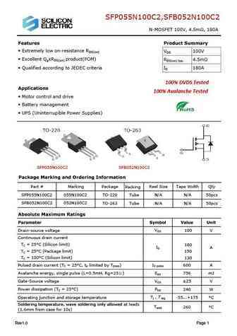
SFP055N100C2,SFB052N100C2 N-MOSFET 100V, 4.5m , 180A Features Product Summary Extremely low on-resistance RDS(on) VDS 100V Excellent QgxRDS(on) product(FOM) RDS(on) typ. 4.5m Qualified according to JEDEC criteria ID 180A 100% DVDS Tested Applications 100% Avalanche Tested Motor control and drive Battery management UPS (Uninterrupible Power Supplies) ... See More ⇒
9.37. Size:2141K cn scilicon
sfp045n100c3 sfb042n100c3.pdf 
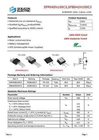
SFP045N100C3,SFB042N100C3 N-MOSFET 100V, 3.9m , 120A Features Product Summary Extremely low on-resistance RDS(on) VDS 100V Excellent QgxRDS(on) product(FOM) RDS(on) typ. 3.9m Qualified according to JEDEC criteria ID R 120A 100% DVDS Tested Applications 100% Avalanche Tested Motor control and drive 100% Avalanche Tested Battery management UPS (Uninter... See More ⇒
9.38. Size:1345K cn scilicon
sfw042n100c3.pdf 
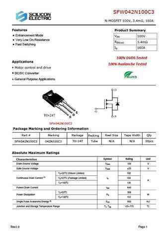
SFW042N100C3 N-MOSFET 100V, 3.4m , 160A Features Product Summary Enhancement Mode VDS 100V Very Low On-Resistance RDS(on) 3.4m Fast Switching ID 160A 100% DVDS Tested Applications 100% Avalanche Tested Motor control and drive 100% Avalanche Tested 100% Avalanche Tested 100% Avalanche Tested 100% Avalanche Tested 100% Avalanche Tested DC/DC C... See More ⇒
9.39. Size:6516K cn scilicon
sfp055n100bc2 sfb052n100bc2.pdf 
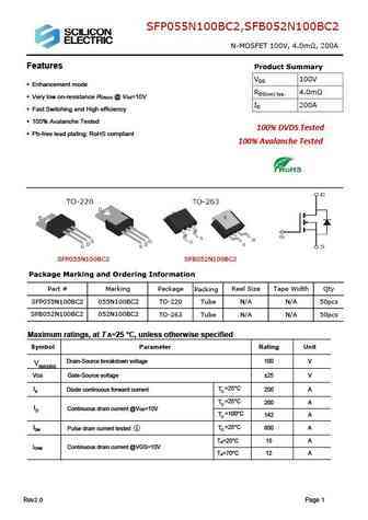
SFP055N100BC2,SFB052N100BC2 N-MOSFET 100V, 4.0m , 200A Features Product Summary VDS 100V Enhancement mode RDS(on) typ. 4.0m Very low on-resistance RDS(on) @ VGS=10V ID 200A Fast Switching and High efficiency 100% Avalanche Tested 100% DVDS Tested Pb-free lead plating; RoHS compliant 100% Avalanche Tested SFP055N100BC2 SFB052N100BC2 Package Marking and ... See More ⇒
9.40. Size:5032K cn scilicon
sfp055n100ac2 sfb052n100ac2.pdf 
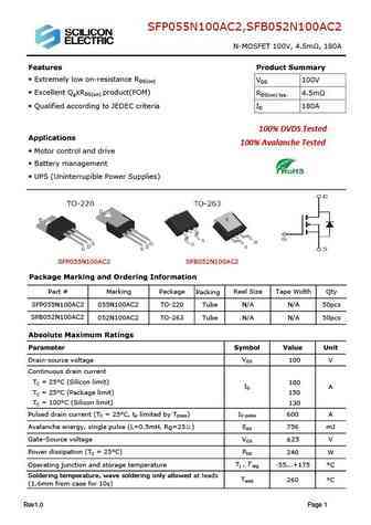
SFP055N100AC2,SFB052N100AC2 N-MOSFET 100V, 4.5m , 180A Features Product Summary Extremely low on-resistance RDS(on) VDS 100V Excellent QgxRDS(on) product(FOM) RDS(on) typ. 4.5m Qualified according to JEDEC criteria ID 180A 100% DVDS Tested Applications 100% Avalanche Tested Motor control and drive Battery management UPS (Uninterrupible Power Supplies... See More ⇒
9.41. Size:720K cn scilicon
sfp032n100c3 sfb030n100c3.pdf 
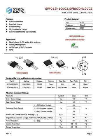
SFP032N100C3,SFB030N100C3 N-MOSFET 100V, 2.6m , 260A Features Product Summary Low on resistance V 100V DS Low gate charge R 2.6m DS(on) typ. Fast switching I 260A D(Silicon Limited) High avalanche current Low reverse transfer capacitances 100% DVDS Tested Application 100% Avalanche Tested Brushed and BLDC Motor drive systems Battery Manag... See More ⇒
9.42. Size:1409K cn scilicon
sfp055n100c3 sfb052n100c3.pdf 
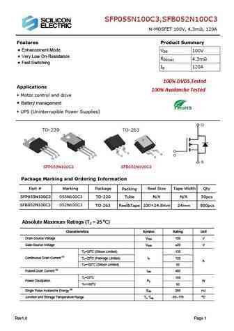
SFP055N100C3,SFB052N100C3 N-MOSFET 100V, 4.3m , 120A Features Product Summary Enhancement Mode VDS 100V Very Low On-Resistance RDS(on) 4.3m Fast Switching ID 120A 100% DVDS Tested Applications 100% Avalanche Tested Motor control and drive 100% Avalanche Tested 100% Avalanche Tested 100% Avalanche Tested 100% Avalanche Tested 100% Avalanche Tested ... See More ⇒
9.43. Size:2137K cn scilicon
sfp045n100bc3 sfb042n100bc3.pdf 
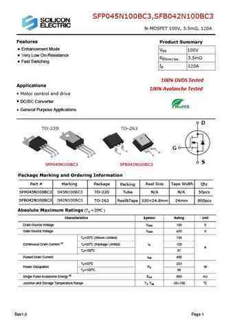
SFP045N100BC3,SFB042N100BC3 N-MOSFET 100V, 3.5m , 120A Features Product Summary Enhancement Mode VDS 100V Very Low On-Resistance RDS(on) typ. 3.5m Fast Switching ID 120A 100% DVDS Tested Applications 100% Avalanche Tested Motor control and drive DC/DC Converter General Purpose Applications D G S SFP045N100BC3 SFB042N100BC3 Package Marking and ... See More ⇒
9.44. Size:309K inchange semiconductor
fqd2n100.pdf 
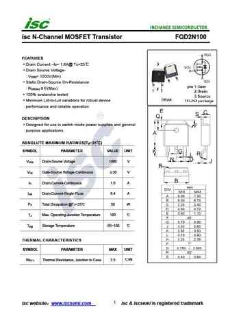
isc N-Channel MOSFET Transistor FQD2N100 FEATURES Drain Current I = 1.6A@ T =25 D C Drain Source Voltage- V = 1000V(Min) DSS Static Drain-Source On-Resistance R 9 (Max) DS(on) 100% avalanche tested Minimum Lot-to-Lot variations for robust device performance and reliable operation DESCRIPTION Designed for use in switch mode power supplies and general purpos... See More ⇒
9.45. Size:208K inchange semiconductor
aod2n100.pdf 
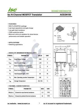
INCHANGE Semiconductor Isc N-Channel MOSFET Transistor AOD2N100 FEATURES With To-252(DPAK) package Low input capacitance and gate charge Low gate input resistance 100% avalanche tested Minimum Lot-to-Lot variations for robust device performance and reliable operation APPLICATIONS Switching applications ABSOLUTE MAXIMUM RATINGS(T =25 ) a SYMBOL PARAMETER VALUE UN... See More ⇒
Detailed specifications: 2G605, 2H1254, 2H1255, 2H1256, 2H1257, 2H1258, 2H1259, 2N100, TIP41, 2N1003, 2N1004, 2N1005, 2N1006, 2N1007, 2N1008, 2N1008A, 2N1008B
Keywords - 2N1000 pdf specs
2N1000 cross reference
2N1000 equivalent finder
2N1000 pdf lookup
2N1000 substitution
2N1000 replacement
![]()
![]()
