BCW30CSM Specs and Replacement
Type Designator: BCW30CSM
Material of Transistor: Si
Polarity: PNP
Absolute Maximum Ratings
Maximum Collector Power Dissipation (Pc): 0.35 W
Maximum Collector-Base Voltage |Vcb|: 40 V
Maximum Collector-Emitter Voltage |Vce|: 32 V
Maximum Emitter-Base Voltage |Veb|: 5 V
Maximum Collector Current |Ic max|: 0.1 A
Max. Operating Junction Temperature (Tj): 150 °C
Electrical Characteristics
Transition Frequency (ft): 150 MHz
Collector Capacitance (Cc): 4 pF
Forward Current Transfer Ratio (hFE), MIN: 120
Noise Figure, dB: -
Package: LCC3
- BJT ⓘ Cross-Reference Search
BCW30CSM datasheet
9.1. Size:451K motorola
bcw29lt1 bcw30lt1.pdf 

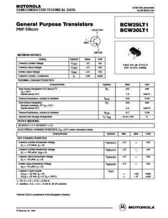
MOTOROLA Order this document SEMICONDUCTOR TECHNICAL DATA by BCW29LT1/D General Purpose Transistors BCW29LT1 PNP Silicon COLLECTOR BCW30LT1 3 1 BASE 3 2 EMITTER 1 MAXIMUM RATINGS 2 Rating Symbol Value Unit Collector Emitter Voltage VCEO 32 Vdc CASE 318 08, STYLE 6 Collector Base Voltage VCBO 32 Vdc SOT 23 (TO 236AB) Emitter Base Voltage VEBO 5.0 Vdc ... See More ⇒
9.2. Size:47K philips
bcw29 bcw30 4.pdf 

DISCRETE SEMICONDUCTORS DATA SHEET book, halfpage M3D088 BCW29; BCW30 PNP general purpose transistors 1999 Apr 13 Product specification Supersedes data of 1997 Sep 03 Philips Semiconductors Product specification PNP general purpose transistors BCW29; BCW30 FEATURES PINNING Low current (max. 100 mA) PIN DESCRIPTION Low voltage (max. 32 V). 1 base 2 emitter APPLICATIONS ... See More ⇒
9.3. Size:111K philips
bcw29 bcw30 2.pdf 

DISCRETE SEMICONDUCTORS DATA SHEET BCW29; BCW30 PNP general purpose transistors Product data sheet 2004 Jan 13 Supersedes data of 1999 Apr 13 NXP Semiconductors Product data sheet PNP general purpose transistors BCW29; BCW30 FEATURES PINNING Low current (max. 100 mA) PIN DESCRIPTION Low voltage (max. 32 V). 1 base 2 emitter APPLICATIONS 3 collector General purpose... See More ⇒
9.4. Size:37K st
bcw30.pdf 

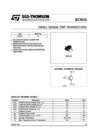
BCW30 SMALL SIGNAL PNP TRANSISTORS Type Marking BCW30 C2 SILICON EPITAXIAL PLANAR PNP TRANSISTORS MINIATURE PLASTIC PACKAGE FOR APPLICATION IN SURFACE MOUNTING 2 CIRCUITS LOW LEVEL AUDIO AMPLIFICATION AND 3 SWITCHING 1 SOT-23 INTERNAL SCHEMATIC DIAGRAM ABSOLUTE MAXIMUM RATINGS Symbol Parameter Value Unit V Collector-Emitter Voltage (V = 0) -32 V CES BE VCEO Collector-Emitt... See More ⇒
9.5. Size:43K fairchild semi
fsbcw30.pdf 

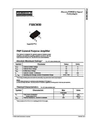
Discrete POWER & Signal Technologies FSBCW30 C E B SuperSOTTM-3 PNP General Purpose Amplifier This device is designed for general purpose medium power amplifiers and switches requiring collector currents to 300 mA. Sourced from Process 68. See BC857A for characteristics. Absolute Maximum Ratings* TA = 25 C unless otherwise noted Symbol Parameter Value Units VCEO Collector-Emitter ... See More ⇒
9.6. Size:45K fairchild semi
bcw30.pdf 

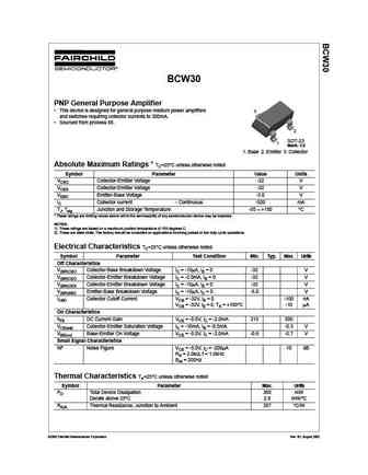
BCW30 PNP General Purpose Amplifier This device is designed for general purpose medium power amplifiers 3 and switches requiring collector currents to 300mA. Sourced from process 68. 2 SOT-23 1 Mark C2 1. Base 2. Emitter 3. Collector Absolute Maximum Ratings * TC=25 C unless otherwise noted Symbol Parameter Value Units VCEO Collector-Emitter Voltage -32 V VCES Collecto... See More ⇒
9.7. Size:309K nxp
bcw29 bcw30.pdf 

Important notice Dear Customer, On 7 February 2017 the former NXP Standard Product business became a new company with the tradename Nexperia. Nexperia is an industry leading supplier of Discrete, Logic and PowerMOS semiconductors with its focus on the automotive, industrial, computing, consumer and wearable application markets In data sheets and application notes which still contain... See More ⇒
9.8. Size:28K diodes
bcw29 bcw30.pdf 

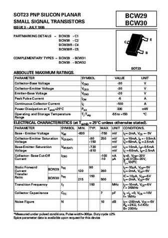
SOT23 PNP SILICON PLANAR BCW29 SMALL SIGNAL TRANSISTORS BCW30 ISSUE 3 - JULY 1995 T I D T I E C B T T SOT23 ABSOLUTE MAXIMUM RATINGS. T V IT II V I V V II i V I V V i V I V V I I i II I Di i i T i T T T ELECTRICAL CHARACTERISTICS (at Tamb = 25 C unless otherwise stated). T I T IT DITI i V I V V I V V II i i V T 8 V I I V I V I I i i V T V I... See More ⇒
9.9. Size:240K onsemi
bcw30lt1-d.pdf 

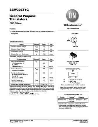
BCW30LT1G General Purpose Transistors PNP Silicon http //onsemi.com Features These Devices are Pb-Free, Halogen Free/BFR Free and are RoHS Compliant COLLECTOR 3 1 BASE MAXIMUM RATINGS Rating Symbol Value Unit 2 EMITTER Collector - Emitter Voltage VCEO -32 Vdc Collector - Base Voltage VCBO -32 Vdc Emitter-Base Voltage VEBO -5.0 Vdc 3 Collector Current - Continuous IC -100 ... See More ⇒
9.10. Size:101K onsemi
bcw30lt1g.pdf 

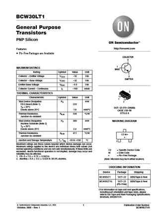
BCW30LT1 General Purpose Transistors PNP Silicon http //onsemi.com Features Pb-Free Packages are Available COLLECTOR 3 1 MAXIMUM RATINGS BASE Rating Symbol Value Unit Collector - Emitter Voltage VCEO -32 Vdc 2 EMITTER Collector - Base Voltage VCBO -32 Vdc Emitter-Base Voltage VEBO -5.0 Vdc Collector Current - Continuous IC -100 mAdc 3 THERMAL CHARACTERISTICS Characteris... See More ⇒
9.11. Size:300K onsemi
bcw30lt1g sbcw30lt1g.pdf 

ON Semiconductor Is Now To learn more about onsemi , please visit our website at www.onsemi.com onsemi and and other names, marks, and brands are registered and/or common law trademarks of Semiconductor Components Industries, LLC dba onsemi or its affiliates and/or subsidiaries in the United States and/or other countries. onsemi owns the rights to a number of patents, trademarks,... See More ⇒
9.12. Size:154K onsemi
sbcw30lt1g.pdf 

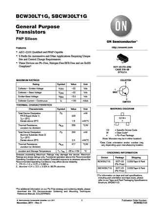
BCW30LT1G, SBCW30LT1G General Purpose Transistors PNP Silicon http //onsemi.com Features AEC-Q101 Qualified and PPAP Capable S Prefix for Automotive and Other Applications Requiring Unique Site and Control Change Requirements These Devices are Pb-Free, Halogen Free/BFR Free and are RoHS Compliant* SOT-23 (TO-236) CASE 318-08 STYLE 6 COLLECTOR MAXIMUM RATINGS 3 Ratin... See More ⇒
9.13. Size:77K cdil
bcw29 bcw30.pdf 

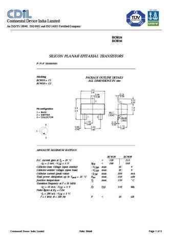
Continental Device India Limited An ISO/TS 16949, ISO 9001 and ISO 14001 Certified Company BCW29 BCW30 SILICON PLANAR EPITAXIAL TRANSISTORS P N P transistors Marking PACKAGE OUTLINE DETAILS BCW29 = C1 ALL DIMENSIONS IN mm BCW30 = C2 Pin configuration 1 = BASE 2 = EMITTER 3 = COLLECTOR 3 1 2 ABSOLUTE MAXIMUM RATINGS BCW29 BCW30 D.C. current gain at Tj = 25 C > 120 215 ... See More ⇒
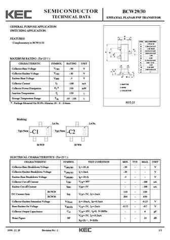
9.14. Size:29K kec
bcw29 bcw30.pdf 

SEMICONDUCTOR BCW29/30 TECHNICAL DATA EPITAXIAL PLANAR PNP TRANSISTOR GENERAL PURPOSE APPLICATION. SWITCHING APPLICATION. E L B L FEATURES DIM MILLIMETERS Complementary to BCW31/32 _ + 2.93 0.20 A B 1.30+0.20/-0.15 C 1.30 MAX 2 3 D 0.45+0.15/-0.05 E 2.40+0.30/-0.20 1 G 1.90 H 0.95 MAXIMUM RATING (Ta=25 ) J 0.13+0.10/-0.05 K 0.00 0.10 CHARACTERISTIC SYMBOL RATING UNIT... See More ⇒
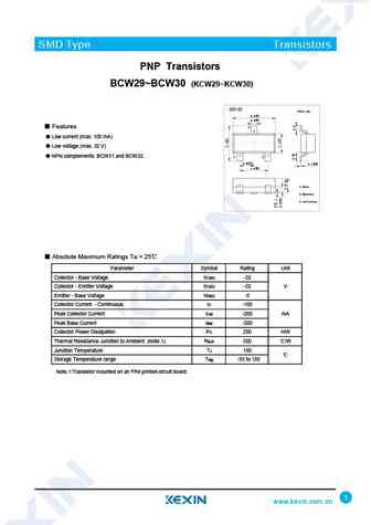
9.15. Size:926K kexin
bcw29 bcw30.pdf 

SMD Type Transistors PNP Transistors BCW29 BCW30 (KCW29 KCW30) SOT-23 Unit mm +0.1 2.9 -0.1 +0.1 0.4-0.1 Features 3 Low current (max. 100 mA) Low voltage (max. 32 V) NPN complements BCW31 and BCW32. 1 2 +0.1 +0.05 0.95 -0.1 0.1 -0.01 +0.1 1.9 -0.1 1.Base 2.Emitter 3.collector Absolute Maximum Ratings Ta = 25 Parameter Symbol Rating Unit Colle... See More ⇒
Detailed specifications: BCW27, BCW28, BCW29, BCW29CSM, BCW29LT1, BCW29LT3, BCW29R, BCW30, TIP31, BCW30LT1, BCW30LT3, BCW30R, BCW31, BCW31CSM, BCW31LT1, BCW31LT3, BCW31R
Keywords - BCW30CSM pdf specs
BCW30CSM cross reference
BCW30CSM equivalent finder
BCW30CSM pdf lookup
BCW30CSM substitution
BCW30CSM replacement
