BCW89R Specs and Replacement
Type Designator: BCW89R
SMD Transistor Code: H31_H6
Material of Transistor: Si
Polarity: PNP
Absolute Maximum Ratings
Maximum Collector Power Dissipation (Pc): 0.2 W
Maximum Collector-Base Voltage |Vcb|: 60 V
Maximum Collector-Emitter Voltage |Vce|: 60 V
Maximum Emitter-Base Voltage |Veb|: 5 V
Maximum Collector Current |Ic max|: 0.1 A
Max. Operating Junction Temperature (Tj): 150 °C
Electrical Characteristics
Transition Frequency (ft): 100 MHz
Collector Capacitance (Cc): 7 pF
Forward Current Transfer Ratio (hFE), MIN: 120
Package: SOT23
BCW89R Substitution
- BJT ⓘ Cross-Reference Search
BCW89R datasheet
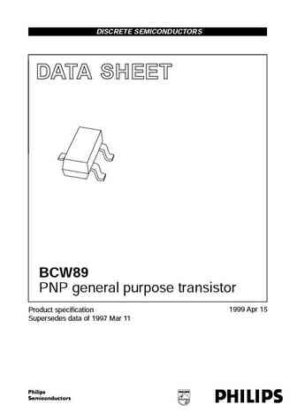
DISCRETE SEMICONDUCTORS DATA SHEET ook, halfpage M3D088 BCW89 PNP general purpose transistor 1999 Apr 15 Product specification Supersedes data of 1997 Mar 11 Philips Semiconductors Product specification PNP general purpose transistor BCW89 FEATURES PINNING Low current (max. 100 mA) PIN DESCRIPTION Low voltage (max. 60 V). 1 base 2 emitter APPLICATIONS 3 collector ... See More ⇒
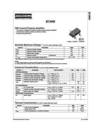
BCW89 PNP General Purpose Amplifier This device is designed for general purpose medium power amplifiers 3 and switches requiring collector currents to 300mA. Sourced from process 68. 2 SOT-23 1 Mark H3 1. Base 2. Emitter 3. Collector Absolute Maximum Ratings * TC=25 C unless otherwise noted Symbol Parameter Value Units VCEO Collector-Emitter Voltage -60 V VCES Collecto... See More ⇒
Important notice Dear Customer, On 7 February 2017 the former NXP Standard Product business became a new company with the tradename Nexperia. Nexperia is an industry leading supplier of Discrete, Logic and PowerMOS semiconductors with its focus on the automotive, industrial, computing, consumer and wearable application markets In data sheets and application notes which still contain... See More ⇒
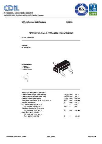
Continental Device India Limited An ISO/TS 16949, ISO 9001 and ISO 14001 Certified Company SOT-23 Formed SMD Package BCW89 SILICON PLANAR EPITAXIAL TRANSISTORS P N P transistors Marking BCW89 = H3 Pin configuration 1 = BASE 2 = EMITTER 3 = COLLECTOR 3 1 2 ABSOLUTE MAXIMUM RATINGS Collector base voltage (open emitter) VCB0 max. 80 V Collector emitter voltage (open base... See More ⇒
Detailed specifications: BCW84, BCW84B, BCW84C, BCW85, BCW86, BCW87, BCW88, BCW89, S8550, BCW90, BCW90A, BCW90B, BCW90C, BCW90K, BCW90KA, BCW90KB, BCW90KC
Keywords - BCW89R pdf specs
BCW89R cross reference
BCW89R equivalent finder
BCW89R pdf lookup
BCW89R substitution
BCW89R replacement
