C103 Specs and Replacement
Type Designator: C103
Material of Transistor: Si
Polarity: PNP
Absolute Maximum Ratings
Maximum Collector Power Dissipation (Pc): 0.25 W
Maximum Collector-Emitter Voltage |Vce|: 6 V
Maximum Collector Current |Ic max|: 0.05 A
Max. Operating Junction Temperature (Tj): 175 °C
Electrical Characteristics
Transition Frequency (ft): 0.6 MHz
Collector Capacitance (Cc): 75 pF
Forward Current Transfer Ratio (hFE), MIN: 15
Package: TO5
C103 Substitution
- BJT ⓘ Cross-Reference Search
C103 datasheet
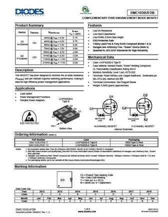
DMC1030UFDB COMPLEMENTARY PAIR ENHANCEMENT MODE MOSFET Product Summary Features ID MAX Low On-Resistance Device V(BR)DSS RDS(ON) max TA = +25 C Low Input Capacitance Low Profile, 0.6mm Max Height 34m @ VGS = 4.5V 5.1A ESD Protected Gate 40m @ VGS = 2.5V 4.7A Q1 12V Totally Lead-Free & Fully RoHS Compliant (Notes 1 & 2) N-Channel 50m @ VGS ... See More ⇒
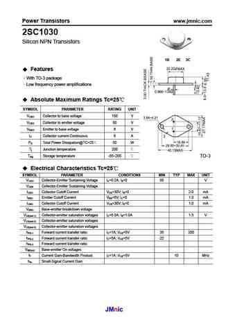
Power Transistors www.jmnic.com 2SC1030 Silicon NPN Transistors 1B 2E 3C Features With TO-3 package Low frequency power amplifications Absolute Maximum Ratings Tc=25 SYMBOL PARAMETER RATING UNIT VCBO Collector to base voltage 150 V VCEO Collector to emitter voltage 80 V VEBO Emitter to base voltage 6 V IC Collector current-Continuous 6 A PD Total Power Dissipation@TC... See More ⇒
krc101s krc102s krc103s krc104s krc105s krc106s.pdf ![]()
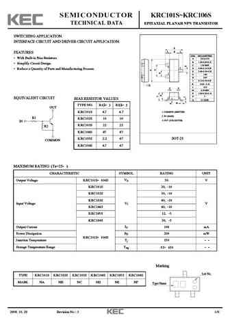
SEMICONDUCTOR KRC101S KRC106S TECHNICAL DATA EPITAXIAL PLANAR NPN TRANSISTOR SWITCHING APPLICATION. INTERFACE CIRCUIT AND DRIVER CIRCUIT APPLICATION. E L B L FEATURES DIM MILLIMETERS With Built-in Bias Resistors. _ + A 2.93 0.20 B 1.30+0.20/-0.15 Simplify Circuit Design. C 1.30 MAX 2 3 D 0.40+0.15/-0.05 Reduce a Quantity of Parts and Manufacturing Process. E 2.40+0.30/... See More ⇒
Detailed specifications: C1, C100, C1001, C1002, C1003, C1004, C101, C102, 2SC5198, C106, C112, C1-12, C118, C119, C12-28, C1-28, C150
Keywords - C103 pdf specs
C103 cross reference
C103 equivalent finder
C103 pdf lookup
C103 substitution
C103 replacement
