2N34 Datasheet. Specs and Replacement
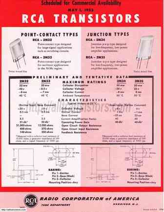
Type Designator: 2N34 📄📄
Material of Transistor: Ge
Polarity: PNP
Absolute Maximum Ratings
Maximum Collector Power Dissipation (Pc): 0.05 W
Maximum Collector-Base Voltage |Vcb|: 40 V
Maximum Collector-Emitter Voltage |Vce|: 25 V
Maximum Collector Current |Ic max|: 0.1 A
Max. Operating Junction Temperature (Tj): 75 °C
Electrical Characteristics
Transition Frequency (ft): 0.2 MHz
Forward Current Transfer Ratio (hFE), MIN: 35
Package: TO22
📄📄 Copy
2N34 Substitution
- BJT ⓘ Cross-Reference Search
2N34 datasheet
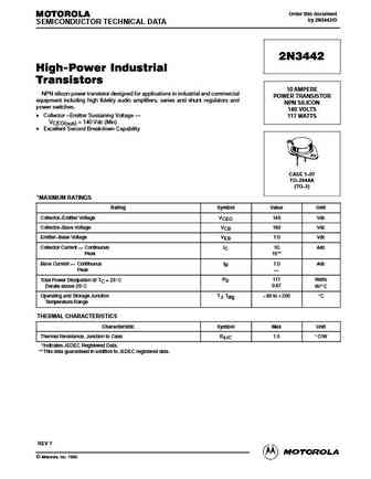
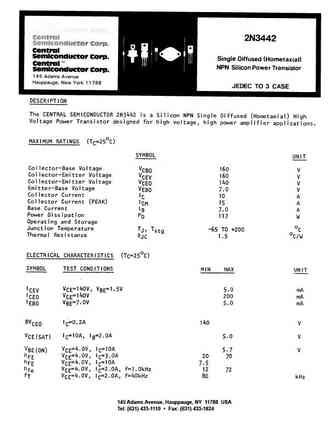
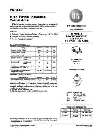
Order this document MOTOROLA by 2N3442/D SEMICONDUCTOR TECHNICAL DATA 2N3442 High-Power Industrial Transistors 10 AMPERE NPN silicon power transistor designed for applications in industrial and commercial POWER TRANSISTOR equipment including high fidelity audio amplifiers, series and shunt regulators and NPN SILICON power switches. 140 VOLTS Collector Emitter Sustaining Vol... See More ⇒
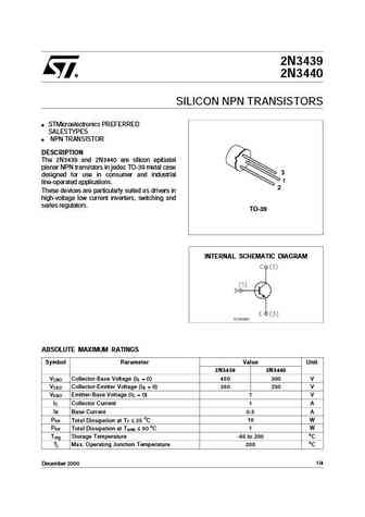
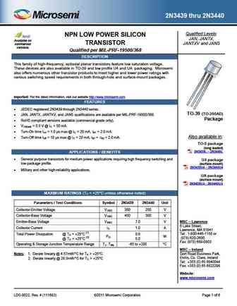
2N3439 2N3440 SILICON NPN TRANSISTORS STMicroelectronics PREFERRED SALESTYPES NPN TRANSISTOR DESCRIPTION The 2N3439 and 2N3440 are silicon epitaxial planar NPN transistors in jedec TO-39 metal case designed for use in consumer and industrial line-operated applications. These devices are particularly suited as drivers in high-voltage low current inverters, switching and seri... See More ⇒
2N3439 2N3440 SILICON NPN TRANSISTORS STMicroelectronics PREFERRED SALESTYPES NPN TRANSISTOR DESCRIPTION The 2N3439 and 2N3440 are silicon epitaxial planar NPN transistors in jedec TO-39 metal case designed for use in consumer and industrial line-operated applications. These devices are particularly suited as drivers in high-voltage low current inverters, switching and seri... See More ⇒
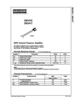
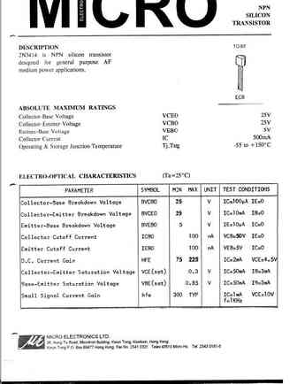
2N3416 2N3417 B TO-92 C E NPN General Purpose Amplifier This device is designed for use as general purpose amplifiers and switches requiring collector currents to 300 mA. Sourced from Process 10. See PN100A for characteristics. Absolute Maximum Ratings* TA = 25 C unless otherwise noted Symbol Parameter Value Units VCEO Collector-Emitter Voltage 50 V VCBO Collector-Base Voltage 50 V... See More ⇒
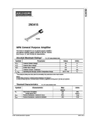
2N3415 B TO-92 C E NPN General Purpose Amplifier This device is designed for use as general purpose amplifiers and switches requiring collector currents to 300 mA. Sourced from Process 10. See PN100A for characteristics. Absolute Maximum Ratings* TA = 25 C unless otherwise noted Symbol Parameter Value Units V Collector-Emitter Voltage 25 V CEO V Collector-Base Voltage 25 V CBO V ... See More ⇒
145 Adams Avenue, Hauppauge, NY 11788 USA Tel (631) 435-1110 Fax (631) 435-1824 ... See More ⇒
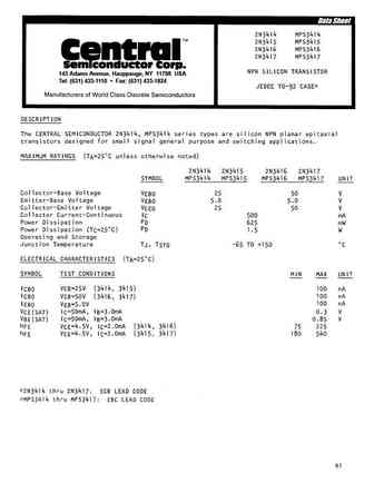
2n3414 2n3415 2n3416 2n3417 mps3414 mps3415 mps3416 mps3417.pdf ![]()
145 Adams Avenue, Hauppauge, NY 11788 USA Tel (631) 435-1110 Fax (631) 435-1824 ... See More ⇒
2N3442 High-Power Industrial Transistors NPN silicon power transistor designed for applications in industrial and commercial equipment including high fidelity audio amplifiers, series and shunt regulators and power switches. http //onsemi.com Features 10 AMPERE Collector -Emitter Sustaining Voltage - VCEO(sus) = 140 Vdc (Min) POWER TRANSISTOR Excellent Second Breakdown Capabi... See More ⇒
2N3442 High-Power Industrial Transistors NPN silicon power transistor designed for applications in industrial and commercial equipment including high fidelity audio amplifiers, series and shunt regulators and power switches. http //onsemi.com Features 10 AMPERE Collector -Emitter Sustaining Voltage - VCEO(sus) = 140 Vdc (Min) POWER TRANSISTOR Excellent Second Breakdown Capabi... See More ⇒
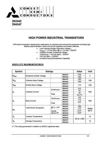
2N3442 2N4347 HIGH POWER INDUSTRIAL TRANSISTORS HIGH POWER INDUSTRIAL TRANSISTORS NPN silicon transistors designed for applications in industrial and commercial equipment including high fidelity audio amplifiers, series and shunts regulators and power switches. Low Collector-Emitter Saturation Voltage VCE(sat) = 1.0 Vdc (Max) @ IC = 2.0 Adc 2N4347 Collector-Emitter Susta... See More ⇒
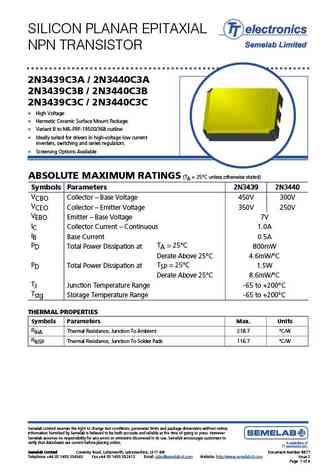
SILICON PLANAR EPITAXIAL NPN TRANSISTOR 2N3439C3A / 2N3440C3A 2N3439C3B / 2N3440C3B 2N3439C3C / 2N3440C3C High Voltage Hermetic Ceramic Surface Mount Package. Variant B to MIL-PRF-19500/368 outline Ideally suited for drivers in high-voltage low current inverters, switching and series regulators. Screening Options Available ABSOLUTE MAXIMUM RATINGS (TA =... See More ⇒
2N3420SMD05 Dimensions in mm (inches). Bipolar NPN Device in a Hermetically sealed 7.54 (0.296) 0.76 (0.030) Ceramic Surface Mount min. 3.175 (0.125) 2.41 (0.095) Package for High 2.41 (0.095) Max. 0.127 (0.005) Reliability Applications 1 3 Bipolar NPN Device. 2 VCEO = 60V IC = 4A 0.127 (0.005) 16 PLCS 0.127 (0.005) 0.50(0.020) 0.50 (0.020) All Semelab herm... See More ⇒
SILICON PLANAR EPITAXIAL NPN TRANSISTOR 2N3439C3A / 2N3440C3A 2N3439C3B / 2N3440C3B 2N3439C3C / 2N3440C3C High Voltage Hermetic Ceramic Surface Mount Package. Variant B to MIL-PRF-19500/368 outline Ideally suited for drivers in high-voltage low current inverters, switching and series regulators. Screening Options Available ABSOLUTE MAXIMUM RATINGS (TA =... See More ⇒
SILICON PLANAR EPITAXIAL NPN TRANSISTOR 2N3439C3A / 2N3440C3A 2N3439C3B / 2N3440C3B 2N3439C3C / 2N3440C3C High Voltage Hermetic Ceramic Surface Mount Package. Variant B to MIL-PRF-19500/368 outline Ideally suited for drivers in high-voltage low current inverters, switching and series regulators. Screening Options Available ABSOLUTE MAXIMUM RATINGS (TA =... See More ⇒
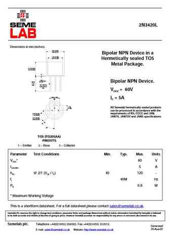
2N3420L Dimensions in mm (inches). 8.51 (0.34) 9.40 (0.37) Bipolar NPN Device in a 7.75 (0.305) 8.51 (0.335) Hermetically sealed TO5 Metal Package. 6.10 (0.240) 6.60 (0.260) 0.89 (0.035)max. 38.00 Bipolar NPN Device. (1.5) 0.41 (0.016) min. 0.53 (0.021) dia. VCEO = 60V 5.08 (0.200) IC = 5A typ. 2.54 All Semelab hermetically sealed products 2 (0.100) 1 3 can b... See More ⇒
SILICON PLANAR EPITAXIAL NPN TRANSISTOR 2N3439C3A / 2N3440C3A 2N3439C3B / 2N3440C3B 2N3439C3C / 2N3440C3C High Voltage Hermetic Ceramic Surface Mount Package. Variant B to MIL-PRF-19500/368 outline Ideally suited for drivers in high-voltage low current inverters, switching and series regulators. Screening Options Available ABSOLUTE MAXIMUM RATINGS (TA =... See More ⇒
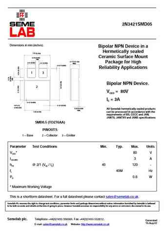
2N3421SMD05 Dimensions in mm (inches). Bipolar NPN Device in a Hermetically sealed 7.54 (0.296) 0.76 (0.030) Ceramic Surface Mount min. 3.175 (0.125) 2.41 (0.095) Package for High 2.41 (0.095) Max. 0.127 (0.005) Reliability Applications 1 3 Bipolar NPN Device. 2 VCEO = 80V IC = 3A 0.127 (0.005) 16 PLCS 0.127 (0.005) 0.50(0.020) 0.50 (0.020) All Semelab herm... See More ⇒
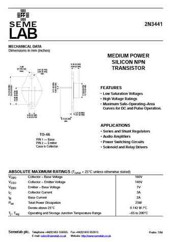
2N3441 SEME LAB MECHANICAL DATA Dimensions in mm (inches) MEDIUM POWER SILICON NPN 6.35 (0.250) 8.64 (0.340) 3.68 (0.145) rad. TRANSISTOR 3.61 (0.142) max. 3.86 (0.145) rad. FEATURES Low Saturation Voltages High Voltage Ratings Maximum Safe Operating Area Curves for DC and Pulse Operation. 1.27 (0.050) 1.91 (0.750) 4.83 (0.190) 5.33 (0.210) 9.14 (0.360)... See More ⇒
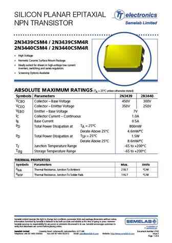
SILICON PLANAR EPITAXIAL NPN TRANSISTOR 2N3439CSM4 / 2N3439CSM4R 2N3440CSM4 / 2N3440CSM4R High Voltage Hermetic Ceramic Surface Mount Package. Ideally suited for drivers in high-voltage low current inverters, switching and series regulators. Screening Options Available ABSOLUTE MAXIMUM RATINGS (TA = 25 C unless otherwise stated) 2N3439 2N3440 Symbols Parame... See More ⇒
2N3420SMD Dimensions in mm (inches). Bipolar NPN Device in a Hermetically sealed 0.89 (0.035) min. Ceramic Surface Mount 3.70 (0.146) 3.70 (0.146) 3.60 (0.142) 3.41 (0.134) 3.41 (0.134) Max. Package for High Reliability Applications 1 3 Bipolar NPN Device. 2 VCEO = 60V IC = 4A 9.67 (0.381) All Semelab hermetically sealed products 9.38 (0.369) 0.50 (0.020) 0.26 (0... See More ⇒
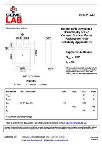
2N3421SMD Dimensions in mm (inches). Bipolar NPN Device in a Hermetically sealed 0.89 (0.035) min. Ceramic Surface Mount 3.70 (0.146) 3.70 (0.146) 3.60 (0.142) 3.41 (0.134) 3.41 (0.134) Max. Package for High Reliability Applications 1 3 Bipolar NPN Device. 2 VCEO = 80V IC = 3A 9.67 (0.381) All Semelab hermetically sealed products 9.38 (0.369) 0.50 (0.020) 0.26 (0... See More ⇒
SILICON PLANAR EPITAXIAL NPN TRANSISTOR 2N3439C3A / 2N3440C3A 2N3439C3B / 2N3440C3B 2N3439C3C / 2N3440C3C High Voltage Hermetic Ceramic Surface Mount Package. Variant B to MIL-PRF-19500/368 outline Ideally suited for drivers in high-voltage low current inverters, switching and series regulators. Screening Options Available ABSOLUTE MAXIMUM RATINGS (TA =... See More ⇒
SILICON PLANAR EPITAXIAL NPN TRANSISTOR 2N3439C3A / 2N3440C3A 2N3439C3B / 2N3440C3B 2N3439C3C / 2N3440C3C High Voltage Hermetic Ceramic Surface Mount Package. Variant B to MIL-PRF-19500/368 outline Ideally suited for drivers in high-voltage low current inverters, switching and series regulators. Screening Options Available ABSOLUTE MAXIMUM RATINGS (TA =... See More ⇒
SILICON PLANAR EPITAXIAL NPN TRANSISTOR 2N3439CSM4 / 2N3439CSM4R 2N3440CSM4 / 2N3440CSM4R High Voltage Hermetic Ceramic Surface Mount Package. Ideally suited for drivers in high-voltage low current inverters, switching and series regulators. Screening Options Available ABSOLUTE MAXIMUM RATINGS (TA = 25 C unless otherwise stated) 2N3439 2N3440 Symbols Parame... See More ⇒
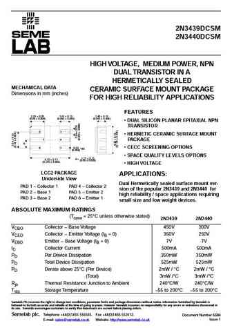
2N3439DCSM 2N3440DCSM HIGH VOLTAGE, MEDIUM POWER, NPN DUAL TRANSISTOR IN A HERMETICALLY SEALED MECHANICAL DATA CERAMIC SURFACE MOUNT PACKAGE Dimensions in mm (inches) FOR HIGH RELIABILITY APPLICATIONS FEATURES 2.29 0.20 1.65 0.13 1.40 0.15 (0.055 0.006) (0.09 0.008) (0.065 0.005) DUAL SILICON PLANAR EPITAXIAL NPN TRANSISTOR 2 3 HERMETIC CERAMIC SURFACE... See More ⇒
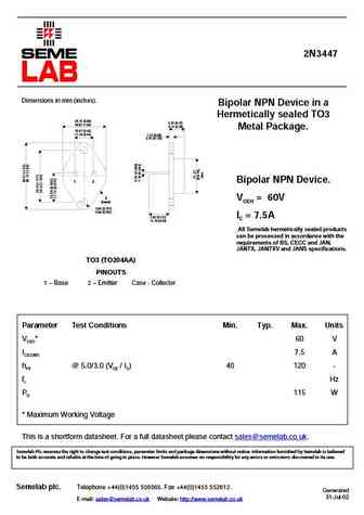
2N3447 Dimensions in mm (inches). Bipolar NPN Device in a Hermetically sealed TO3 25.15 (0.99) 6.35 (0.25) 26.67 (1.05) 9.15 (0.36) Metal Package. 10.67 (0.42) 11.18 (0.44) 1.52 (0.06) 3.43 (0.135) 1 2 Bipolar NPN Device. 3 VCEO = 60V (case) 3.84 (0.151) 4.09 (0.161) 7.92 (0.312) IC = 7.5A 12.70 (0.50) All Semelab hermetically sealed products can be processed in ... See More ⇒
2N3421ASMD05 Dimensions in mm (inches). Bipolar NPN Device in a Hermetically sealed 7.54 (0.296) 0.76 (0.030) Ceramic Surface Mount min. 3.175 (0.125) 2.41 (0.095) Package for High 2.41 (0.095) Max. 0.127 (0.005) Reliability Applications 1 3 Bipolar NPN Device. 2 VCEO = 80V IC = 5A 0.127 (0.005) 16 PLCS 0.127 (0.005) 0.50(0.020) 0.50 (0.020) All Semelab her... See More ⇒
2N3445 Dimensions in mm (inches). Bipolar NPN Device in a Hermetically sealed TO3 25.15 (0.99) 6.35 (0.25) 26.67 (1.05) 9.15 (0.36) Metal Package. 10.67 (0.42) 11.18 (0.44) 1.52 (0.06) 3.43 (0.135) 1 2 Bipolar NPN Device. 3 VCEO = 60V (case) 3.84 (0.151) 4.09 (0.161) 7.92 (0.312) IC = 7.5A 12.70 (0.50) All Semelab hermetically sealed products can be processed in ... See More ⇒
2N3421ASMD Dimensions in mm (inches). Bipolar NPN Device in a Hermetically sealed 0.89 (0.035) min. Ceramic Surface Mount 3.70 (0.146) 3.70 (0.146) 3.60 (0.142) 3.41 (0.134) 3.41 (0.134) Max. Package for High Reliability Applications 1 3 Bipolar NPN Device. 2 VCEO = 80V IC = 5A 9.67 (0.381) All Semelab hermetically sealed products 9.38 (0.369) 0.50 (0.020) 0.26 (... See More ⇒
2N3439DCSM 2N3440DCSM HIGH VOLTAGE, MEDIUM POWER, NPN DUAL TRANSISTOR IN A HERMETICALLY SEALED MECHANICAL DATA CERAMIC SURFACE MOUNT PACKAGE Dimensions in mm (inches) FOR HIGH RELIABILITY APPLICATIONS FEATURES 2.29 0.20 1.65 0.13 1.40 0.15 (0.055 0.006) (0.09 0.008) (0.065 0.005) DUAL SILICON PLANAR EPITAXIAL NPN TRANSISTOR 2 3 HERMETIC CERAMIC SURFACE... See More ⇒
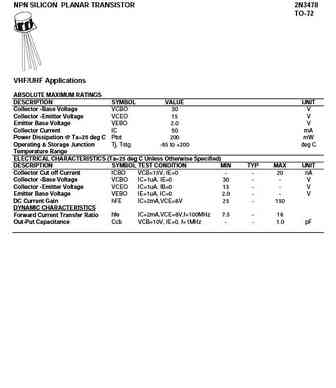
IS / IECQC 700000 IS/ISO 9002 IS / IECQC 750100 Lic# QSC/L- 000019.2 Continental Device India Limited An IS/ISO 9002 and IECQ Certified Manufacturer NPN SILICON PLANAR TRANSISTOR 2N3478 TO-72 Boca Semiconductor Corp. BSC VHF/UHF Applications ABSOLUTE MAXIMUM RATINGS DESCRIPTION SYMBOL VALUE UNIT Collector -Base Voltage VCBO 30 V Collector -Emitter Voltage VCEO 15 V Emitter Base... See More ⇒
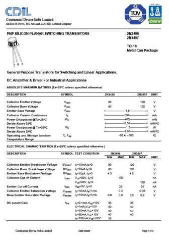
Continental Device India Limited Q An ISO/TS 16949, ISO 9001 and ISO 14001 Certified Company PNP SILICON PLANAR SWITCHING TRANSISTORS 2N3496 2N3497 TO-18 Metal Can Package General Purpose Transistors for Switching and Linear Applications. DC Amplilfier & Driver For Industrial Applications ABSOLUTE MAXIMUM RATINGS (Ta=25 C unless specified otherwise) DESCRIPTION SYMBOL 2N3496 2N3497 ... See More ⇒
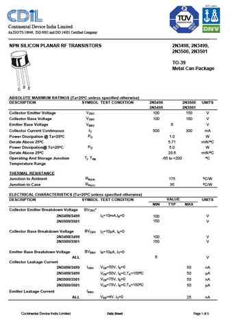
Continental Device India Limited An ISO/TS 16949, ISO 9001 and ISO 14001 Certified Company NPN SILICON PLANAR RF TRANSISTORS 2N3498, 2N3499, 2N3500, 2N3501 TO-39 Metal Can Package ABSOLUTE MAXIMUM RATINGS (Ta=25 C unless specified otherwise) DESCRIPTION SYMBOL TEST CONDITION 2N3498 2N3500 UNITS 2N3499 2N3501 VCEO Collector Emitter Voltage 100 150 V VCBO Collector Base Voltage 100 ... See More ⇒
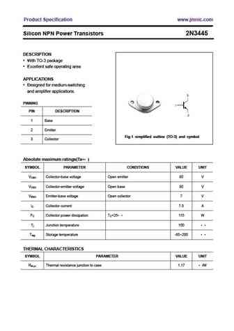
Product Specification www.jmnic.com Silicon NPN Power Transistors 2N3445 DESCRIPTION With TO-3 package Excellent safe operating area APPLICATIONS Designed for medium-switching and amplifier applications. PINNING PIN DESCRIPTION 1 Base 2 Emitter Fig.1 simplified outline (TO-3) and symbol 3 Collector Absolute maximum ratings(Ta= ) SYMBOL PARAMETER CONDITIONS VALU... See More ⇒
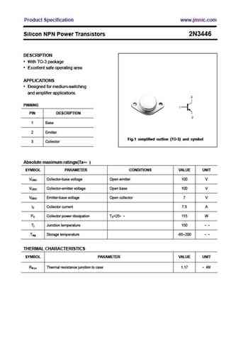
Product Specification www.jmnic.com Silicon NPN Power Transistors 2N3446 DESCRIPTION With TO-3 package Excellent safe operating area APPLICATIONS Designed for medium-switching and amplifier applications. PINNING PIN DESCRIPTION 1 Base 2 Emitter Fig.1 simplified outline (TO-3) and symbol 3 Collector Absolute maximum ratings(Ta= ) SYMBOL PARAMETER CONDITIONS VALU... See More ⇒
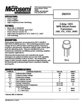
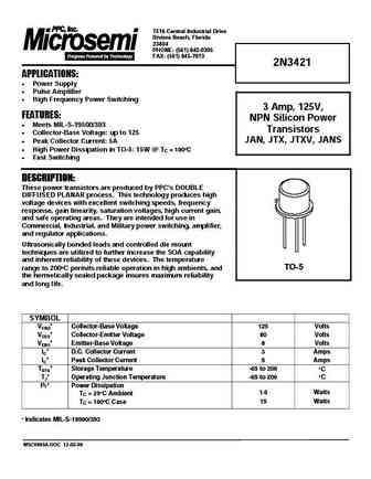
7516 Central Industrial Drive Riviera Beach, Florida 33404 PHONE (561) 842-0305 FAX (561) 845-7813 2N3419 APPLICATIONS Power Supply Pulse Amplifier High Frequency Power Switching 3 Amp, 125V, FEATURES NPN Silicon Power Meets MIL-S-19500/393 Transistors Collector-Base Voltage up to 125V JAN, JTX, JTXV, JANS Peak Collector Current 5A High Power ... See More ⇒
7516 Central Industrial Drive Riviera Beach, Florida 33404 PHONE (561) 842-0305 FAX (561) 845-7813 2N3420 APPLICATIONS Power Supply Pulse Amplifier High Frequency Power Switching 3 Amp, 85V, FEATURES NPN Silicon Power Meets MIL-S-19500/393 Transistors Collector-Base Voltage up to 85 JAN, JTX, JTXV, JANS Peak Collector Current 5A High Power Dis... See More ⇒
2N3439 thru 2N3440 Qualified Levels NPN LOW POWER SILICON JAN, JANTX, Available on TRANSISTOR JANTXV and JANS commercial versions Qualified per MIL-PRF-19500/368 DESCRIPTION This family of high-frequency, epitaxial planar transistors feature low saturation voltage. These devices are also available in TO-39 and low profile U4 and UA packaging. Microsemi also offers nume... See More ⇒
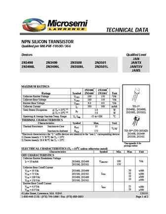
2n3498 2n3499 2n3450 2n3451.pdf ![]()
TECHNICAL DATA NPN SILICON TRANSISTOR Qualified per MIL-PRF-19500/366 Devices Qualified Level JAN 2N3498 2N3499 2N3500 2N3501 JANTX 2N3498L 2N3499L 2N3500L 2N3501L JANTXV JANS MAXIMUM RATINGS 2N3498* 2N3500* Ratings Symbol 2N3499* 2N3501* Unit Collector-Emitter Voltage 100 150 Vdc VCEO Collector-Base Voltage 100 150 Vdc VCBO Emitter-Base Voltage 6.0 6.0 Vdc VE... See More ⇒
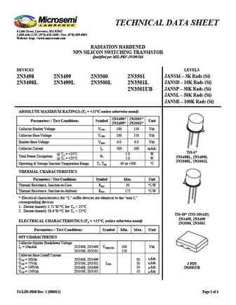
TECHNICAL DATA SHEET 6 Lake Street, Lawrence, MA 01841 1-800-446-1158 / (978) 620-2600 / Fax (978) 689-0803 Website http //www.microsemi.com RADIATION HARDENED NPN SILICON SWITCHING TRANSISTOR Qualified per MIL-PRF-19500/366 DEVICES LEVELS JANSM 3K Rads (Si) 2N3498 2N3499 2N3500 2N3501 JANSD 10K Rads (Si) 2N3498L 2N3499L 2N3500L 2N3501L JANSP 30K Rads (Si) ... See More ⇒
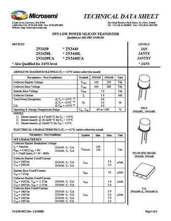
TECHNICAL DATA SHEET 6 Lake Street, Lawrence, MA 01841 Gort Road Business Park, Ennis, Co. Clare, Ireland 1-800-446-1158 / (978) 620-2600 / Fax (978) 689-0803 Tel +353 (0) 65 6840044 Fax +353 (0) 65 6822298 Website http //www.microsemi.com NPN LOW POWER SILICON TRANSISTOR Qualified per MIL-PRF-19500/368 DEVICES LEVELS JAN 2N3439 * 2N3440 JANTX 2N3439L * 2N3440L JANTXV ... See More ⇒
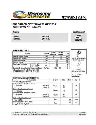
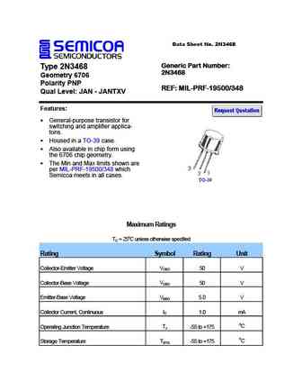
TECHNICAL DATA PNP SILICON SWITCHING TRANSISTOR Qualified per MIL-PRF-19500/348 Devices Qualified Level JAN 2N3467 2N3468 JANTX 2N3467L 2N3468L JANTXV MAXIMUM RATINGS 2N3467 2N3468 Ratings Symbol Unit 2N3467L 2N3468L Collector-Emitter Voltage 40 50 Vdc VCEO TO-39* (TO-205AD) Collector-Base Voltage 40 50 Vdc VCBO 2N3467, 2N3468 Emitter-Base Voltage 5.0 Vdc ... See More ⇒
7516 Central Industrial Drive Riviera Beach, Florida 33404 PHONE (561) 842-0305 FAX (561) 845-7813 2N3421 APPLICATIONS Power Supply Pulse Amplifier High Frequency Power Switching 3 Amp, 125V, FEATURES NPN Silicon Power Meets MIL-S-19500/393 Transistors Collector-Base Voltage up to 125 JAN, JTX, JTXV, JANS Peak Collector Current 5A High Power D... See More ⇒
TECHNICAL DATA SHEET 6 Lake Street, Lawrence, MA 01841 1-800-446-1158 / (978) 620-2600 / Fax (978) 689-0803 Website http //www.microsemi.com RADIATION HARDENED NPN SILICON SWITCHING TRANSISTOR Qualified per MIL-PRF-19500/366 DEVICES LEVELS JANSM 3K Rads (Si) 2N3498 2N3499 2N3500 2N3501 JANSD 10K Rads (Si) 2N3498L 2N3499L 2N3500L 2N3501L JANSP 30K Rads (Si) ... See More ⇒
7516 Central Industrial Drive Riviera Beach, Florida 33404 PHONE (561) 842-0305 FAX (561) 845-7813 2N3418 APPLICATIONS Power Supply Pulse Amplifier High Frequency Power Switching 3 Amp, 85V, FEATURES NPN Silicon Power Meets MIL-S-19500/393 Transistors Collector-Base Voltage up to 85V JAN, JTX, JTXV, JANS Peak Collector Current 5A High Power Di... See More ⇒
TECHNICAL DATA PNP SILICON SWITCHING TRANSISTOR Qualified per MIL-PRF-19500/348 Devices Qualified Level JAN 2N3467 2N3468 JANTX 2N3467L 2N3468L JANTXV MAXIMUM RATINGS 2N3467 2N3468 Ratings Symbol Unit 2N3467L 2N3468L Collector-Emitter Voltage 40 50 Vdc VCEO TO-39* (TO-205AD) Collector-Base Voltage 40 50 Vdc VCBO 2N3467, 2N3468 Emitter-Base Voltage 5.0 Vdc ... See More ⇒
TECHNICAL DATA SHEET 6 Lake Street, Lawrence, MA 01841 Gort Road Business Park, Ennis, Co. Clare, Ireland 1-800-446-1158 / (978) 620-2600 / Fax (978) 689-0803 Tel +353 (0) 65 6840044 Fax +353 (0) 65 6822298 Website http //www.microsemi.com NPN LOW POWER SILICON TRANSISTOR Qualified per MIL-PRF-19500/368 DEVICES LEVELS JAN 2N3439 * 2N3440 JANTX 2N3439L * 2N3440L JANTXV ... See More ⇒
Data Sheet No. 2N3468 Generic Part Number Type 2N3468 2N3468 Geometry 6706 Polarity PNP REF MIL-PRF-19500/348 Qual Level JAN - JANTXV Features General-purpose transistor for switching and amplifier applica- tons. Housed in a TO-39 case. Also available in chip form using the 6706 chip geometry. The Min and Max limits shown are per MIL-PRF-19500/348 which Semi... See More ⇒
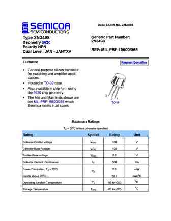
Data Sheet No. 2N3498 Generic Part Number Type 2N3498 2N3498 Geometry 5620 Polarity NPN REF MIL-PRF-19500/366 Qual Level JAN - JANTXV Features General-purpose silicon transistor for switching and amplifier appli- cations. Housed in TO-39 case. Also available in chip form using the 5620 chip geometry. The Min and Max limits shown are per MIL-PRF-19500/366 whic... See More ⇒
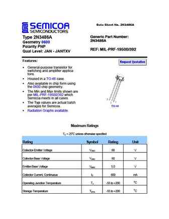
Data Sheet No. 2N3486A Generic Part Number Type 2N3486A 2N3486A Geometry 0600 Polarity PNP REF MIL-PRF-19500/392 Qual Level JAN - JANTXV Features General-purpose transistor for switching and amplifier applica- tons. Housed in a TO-46 case. Also available in chip form using the 0600 chip geometry. The Min and Max limits shown are per MIL-PRF-19500/392 which S... See More ⇒
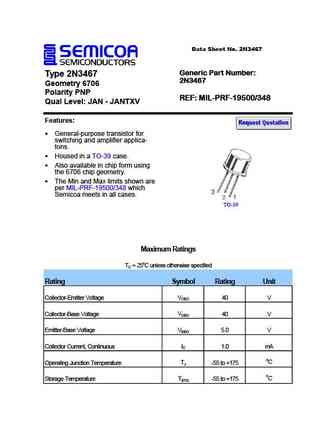
Data Sheet No. 2N3467 Generic Part Number Type 2N3467 2N3467 Geometry 6706 Polarity PNP REF MIL-PRF-19500/348 Qual Level JAN - JANTXV Features General-purpose transistor for switching and amplifier applica- tons. Housed in a TO-39 case. Also available in chip form using the 6706 chip geometry. The Min and Max limits shown are per MIL-PRF-19500/348 which Semi... See More ⇒
Data Sheet No. 2N3485A Generic Part Number Type 2N3485A 2N3485A Geometry 0600 Polarity PNP REF MIL-PRF-19500/392 Qual Level JAN - JANTXV Features General-purpose transistor for switching and amplifier applica- tons. Housed in a TO-46 case. Also available in chip form using the 0600 chip geometry. The Min and Max limits shown are per MIL-PRF-19500/392 which S... See More ⇒
2n3418 2n3419 2n3420 2n3421.pdf ![]()
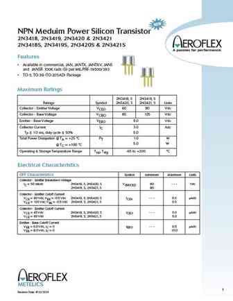
NPN Meduim Power Silicon Transistor 2N3418, 2N3419, 2N3420 & 2N3421 2N3418S, 2N3419S, 2N3420S & 2N3421S Features Available in commercial, JAN, JANTX, JANTXV, JANS and JANSR 100K rads (Si) per MIL-PRF-19500/393 TO-5, TO-39 (TO-205AD) Package Maximum Ratings 2N3418, S 2N3419, S Ratings Symbol 2N3420, S 2N3421, S Units Collector - Emitter Voltage VCEO 60 80 Vdc Collector - Base... See More ⇒
... See More ⇒
... See More ⇒
Inchange Semiconductor Product Specification Silicon NPN Power Transistors 2N3448 DESCRIPTION With TO-3 package Excellent Safe Operating Area APPLICATIONS Designed for medium-switching and amplifier applications. PINNING PIN DESCRIPTION 1 Base 2 Emitter Fig.1 simplified outline (TO-3) and symbol 3 Collector ABSOLUTE MAXIMUM RATINGS(Ta=25 ) SYMBOL PARAMETER CON... See More ⇒
Inchange Semiconductor Product Specification Silicon NPN Power Transistors 2N3441 DESCRIPTION With TO-66 package Continuous collector current-IC=3A Power dissipation -PD=25W @TC=25 APPLICATIONS For use in general-purpose switching and Linear amplifier applications such as Driver for high power outputs Series and shunt regulators Audio and servo amplifiers ... See More ⇒
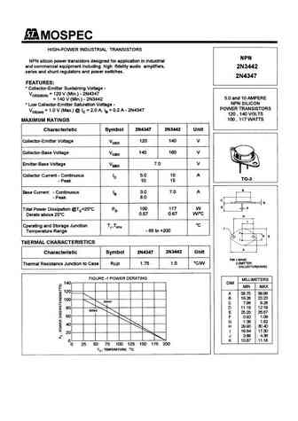
Inchange Semiconductor Product Specification Silicon NPN Power Transistors 2N3442 DESCRIPTION With TO-3 package Excellent safe operating area APPLICATIONS For industrial and commercial equipment including high fidelity audio amplifiers, series and shunt regulators and power switches applications PINNING PIN DESCRIPTION 1 Base 2 Emitter Fig.1 simplified outline (T... See More ⇒
Inchange Semiconductor Product Specification Silicon NPN Power Transistors 2N3447 DESCRIPTION With TO-3 package Excellent safe operating area APPLICATIONS Designed for medium-switching and amplifier applications. PINNING PIN DESCRIPTION 1 Base 2 Emitter Fig.1 simplified outline (TO-3) and symbol 3 Collector ABSOLUTE MAXIMUM RATINGS(Ta=25 ) SYMBOL PARAMETER CON... See More ⇒
Inchange Semiconductor Product Specification Silicon NPN Power Transistors 2N3445 DESCRIPTION With TO-3 package Excellent safe operating area APPLICATIONS Designed for medium-switching and amplifier applications. PINNING PIN DESCRIPTION 1 Base 2 Emitter Fig.1 simplified outline (TO-3) and symbol 3 Collector Absolute maximum ratings(Ta= ) SYMBOL PARAMETER CONDI... See More ⇒
Inchange Semiconductor Product Specification Silicon NPN Power Transistors 2N3446 DESCRIPTION With TO-3 package Excellent safe operating area APPLICATIONS Designed for medium-switching and amplifier applications. PINNING PIN DESCRIPTION 1 Base 2 Emitter Fig.1 simplified outline (TO-3) and symbol 3 Collector Absolute maximum ratings(Ta= ) SYMBOL PARAMETER CONDI... See More ⇒
Detailed specifications: 2N3394, 2N3394U, 2N3395, 2N3396, 2N3397, 2N3398, 2N3399, 2N339A, 2SC2625, 2N340, 2N3400, 2N3401, 2N3402, 2N3403, 2N3404, 2N3405, 2N3407
Keywords - 2N34 pdf specs
2N34 cross reference
2N34 equivalent finder
2N34 pdf lookup
2N34 substitution
2N34 replacement
BJT Parameters and How They Relate
History: 2N336A
🌐 : EN ES РУ
LIST
Last Update
BJT: ZDT6705 | GA1L4Z | GA1A4M | SBT42 | 2SA200-Y | 2SA200-O
Popular searches
2sa970 | a970 | d2390 transistor | 2n5087 equivalent | tip147 datasheet | 2n4124 | mj15022 | toshiba c5198
