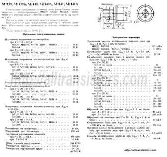
MP40 Specs and Replacement
Type Designator: MP40
Material of Transistor: Ge
Polarity: PNP
Absolute Maximum Ratings
Maximum Collector Power Dissipation (Pc): 0.15 W
Maximum Collector-Base Voltage |Vcb|: 15 V
Maximum Collector-Emitter Voltage |Vce|: 15 V
Maximum Emitter-Base Voltage |Veb|: 5 V
Maximum Collector Current |Ic max|: 0.15 A
Max. Operating Junction Temperature (Tj): 85 °C
Electrical Characteristics
Transition Frequency (ft): 1 MHz
Forward Current Transfer Ratio (hFE), MIN: 20
Noise Figure, dB: -
MP40 Substitution
- BJT ⓘ Cross-Reference Search
MP40 datasheet
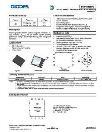
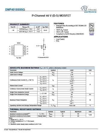
DMP4015SPS Green 40V P-CHANNEL ENHANCEMENT MODE MOSFET POWERDI Product Summary Features and Benefits 100% Unclamped Inductive Switch (UIS) Test In Production ID V(BR)DSS RDS(on) max TA = +25 C Low On-Resistance Fast Switching Speed 11m @ VGS = -10V -17A -40V Lead-Free Finish; RoHS Compliant (Notes 1 & 2) 15m @ VGS = -4.5V -14.5A Halogen and... See More ⇒
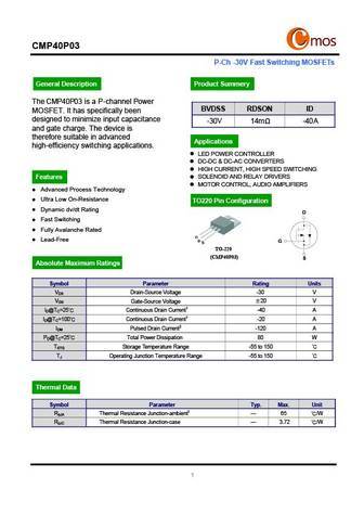
CMP40P03 P-Ch -30V Fast Switching MOSFETs General Description Product Summery The CMP40P03 is a P-channel Power BVDSS RDSON ID MOSFET. It has specifically been designed to minimize input capacitance -30V 14m -40A and gate charge. The device is therefore suitable in advanced Applications high-efficiency switching applications. LED POWER CONTROLLER DC-DC & DC-AC CONVERTERS ... See More ⇒
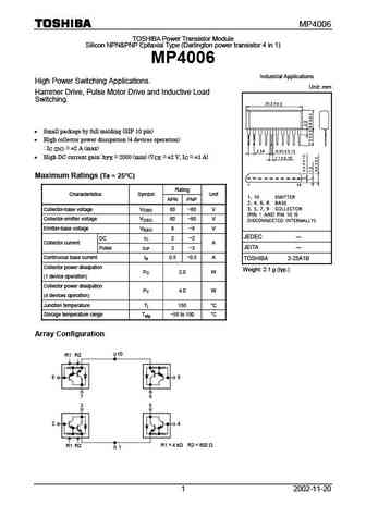
MP4006 TOSHIBA Power Transistor Module Silicon NPN&PNP Epitaxial Type (Darlington power transistor 4 in 1) MP4006 Industrial Applications High Power Switching Applications. Unit mm Hammer Drive, Pulse Motor Drive and Inductive Load Switching. Small package by full molding (SIP 10 pin) High collector power dissipation (4 devices operation) I = 2 A (max) C (DC)... See More ⇒
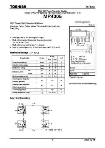
MP4005 TOSHIBA Power Transistor Module Silicon NPN&PNP Epitaxial Type (Darlington power transistor 4 in 1) MP4005 Industrial Applications High Power Switching Applications. Unit mm Hammer Drive, Pulse Motor Drive and Inductive Load Switching. Small package by full molding (SIP 10 pin) High collector power dissipation (4 devices operation) P = 4 W (Ta = 25 C) T... See More ⇒

MP4020 TOSHIBA Power Transistor Module Silicon NPN Epitaxial Type (Darlington power transistor 4 in 1) MP4020 Industrial Applications High Power Switching Applications. Unit mm Hammer Drive, Pulse Motor Drive and Inductive Load Switching. Small package by full molding (SIP 10 pin) High collector power dissipation (4 devices operation) P = 4 W (Ta = 25 C) T ... See More ⇒
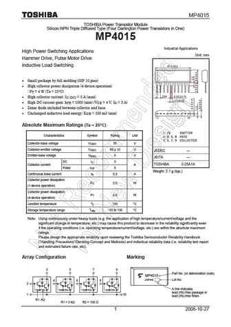
MP4015 TOSHIBA Power Transistor Module Silicon NPN Triple Diffused Type (Four Darlington Power Transistors in One) MP4015 Industrial Applications High Power Switching Applications Unit mm Hammer Drive, Pulse Motor Drive Inductive Load Switching Small package by full molding (SIP 10 pins) High collector power dissipation (4-device operation) PT = 4 W (Ta = 25 C) ... See More ⇒
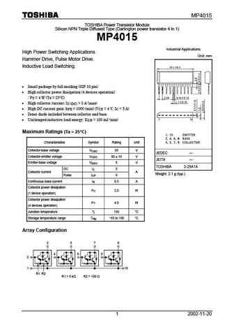
MP4015 TOSHIBA Power Transistor Module Silicon NPN Triple Diffused Type (Darlington power transistor 4 in 1) MP4015 Industrial Applications High Power Switching Applications. Unit mm Hammer Drive, Pulse Motor Drive. Inductive Load Switching. Small package by full molding (SIP 10 pin) High collector power dissipation (4 devices operation) P = 4 W (Ta = 25 C) T ... See More ⇒
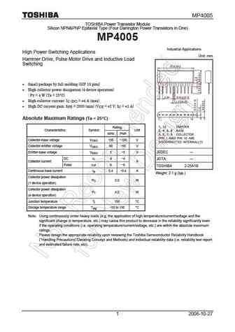
MP4005 TOSHIBA Power Transistor Module Silicon NPN&PNP Epitaxial Type (Four Darlington Power Transistors in One) MP4005 Industrial Applications High Power Switching Applications Unit mm Hammer Drive, Pulse Motor Drive and Inductive Load Switching Small package by full molding (SIP 10 pins) High collector power dissipation (4-device operation) PT = 4 W (Ta = 25 C... See More ⇒
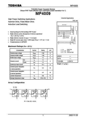
MP4009 TOSHIBA Power Transistor Module Silicon PNP Triple Diffused Type (Darlington power transistor 4 in 1) MP4009 Industrial Applications High Power Switching Applications. Unit mm Hammer Drive, Pulse Motor Drive. Inductive Load Switching. Small package by full molding (SIP 10 pin) High collector power dissipation (4 devices operation) P = 4 W (Ta = 25 C) T ... See More ⇒
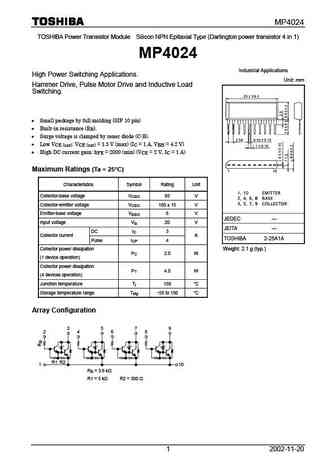
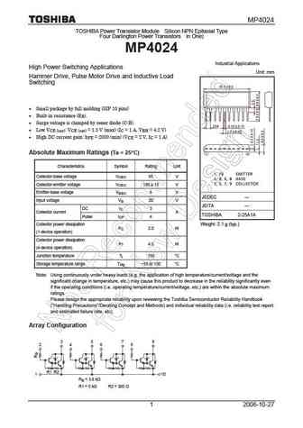
MP4024 TOSHIBA Power Transistor Module Silicon NPN Epitaxial Type (Darlington power transistor 4 in 1) MP4024 Industrial Applications High Power Switching Applications. Unit mm Hammer Drive, Pulse Motor Drive and Inductive Load Switching. Small package by full molding (SIP 10 pin) Built-in resistance (R ). B Surge voltage is clamped by zener diode (C-B). ... See More ⇒

MP4013 TOSHIBA Power Transistor Module Silicon NPN Epitaxial Type (Darlington power transistor 4 in 1) MP4013 Industrial Applications High Power Switching Applications. Unit mm Hammer Drive, Pulse Motor Drive and Inductive Load Switching. Small package by full molding (SIP 10 pin) High collector power dissipation (4 devices operation) P = 4 W (Ta = 25 C) T ... See More ⇒
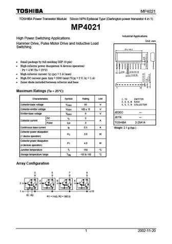
MP4021 TOSHIBA Power Transistor Module Silicon NPN Epitaxial Type (Darlington power transistor 4 in 1) MP4021 Industrial Applications High Power Switching Applications. Unit mm Hammer Drive, Pulse Motor Drive and Inductive Load Switching. Small package by full molding (SIP 10 pin) High collector power dissipation (4 devices operation) P = 4 W (Ta = 25 C) T ... See More ⇒
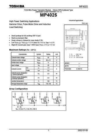
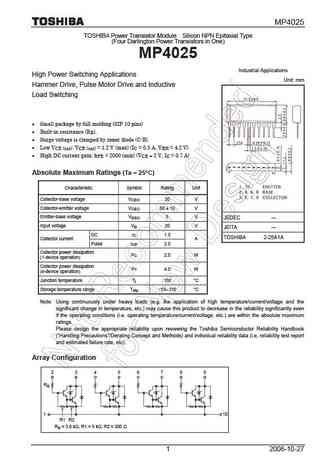
MP4025 TOSHIBA Power Transistor Module Silicon NPN Epitaxial Type (darlington power transistor 4 in 1) MP4025 Industrial Applications High Power Switching Applications Unit mm Hammer Drive, Pulse Motor Drive and Inductive Load Switching Small package by full molding (SIP 10 pin) Built-in resistance (RB). Surge voltage is clamped by zener diode (C-B). Low ... See More ⇒

MP4013 TOSHIBA Power Transistor Module Silicon NPN Epitaxial Type (Four Darlington Power Transistors 4 in One) MP4013 Industrial Applications High Power Switching Applications Unit mm Hammer Drive, Pulse Motor Drive and Inductive Load Switching Small package by full molding (SIP 10 pins) High collector power dissipation (4-device operation) PT = 4 W (Ta = 25 C) ... See More ⇒
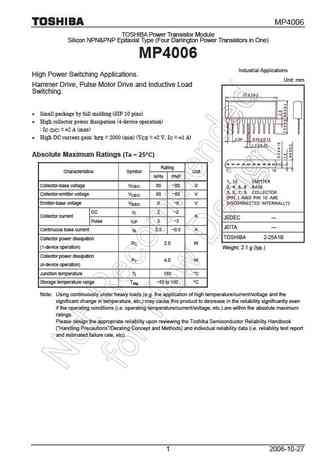
MP4006 TOSHIBA Power Transistor Module Silicon NPN&PNP Epitaxial Type (Four Darlington Power Transistors in One) MP4006 Industrial Applications High Power Switching Applications. Unit mm Hammer Drive, Pulse Motor Drive and Inductive Load Switching. Small package by full molding (SIP 10 pins) High collector power dissipation (4-device operation) IC (DC) = 2 A (m... See More ⇒
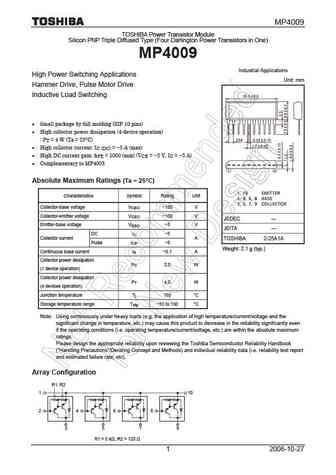
MP4009 TOSHIBA Power Transistor Module Silicon PNP Triple Diffused Type (Four Darlington Power Transistors in One) MP4009 Industrial Applications High Power Switching Applications Unit mm Hammer Drive, Pulse Motor Drive Inductive Load Switching Small package by full molding (SIP 10 pins) High collector power dissipation (4-device operation) PT = 4 W (Ta = 25 C) ... See More ⇒

MP4021 TOSHIBA Power Transistor Module Silicon NPN Epitaxial Type (Four Darlington Power Transistors in One) MP4021 Industrial Applications High Power Switching Applications Unit mm Hammer Drive, Pulse Motor Drive and Inductive Load Switching Small package by full molding (SIP 10 pins) High collector power dissipation (4-device operation) PT = 4 W (Ta = 25 C) ... See More ⇒
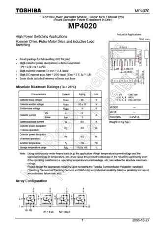
MP4020 TOSHIBA Power Transistor Module Silicon NPN Epitaxial Type (Fourd Darlington Power tTransistors in One) MP4020 Industrial Applications High Power Switching Applications Unit mm Hammer Drive, Pulse Motor Drive and Inductive Load Switching Small package by full molding (SIP 10 pins) High collector power dissipation (4-device operation) PT = 4 W (Ta = 25 C) ... See More ⇒
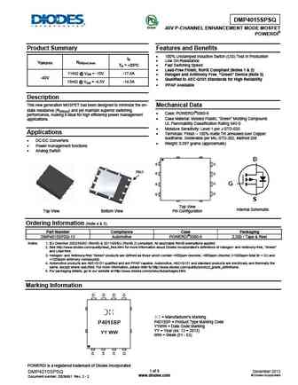
DMP4015SPSQ Green 40V P-CHANNEL ENHANCEMENT MODE MOSFET POWERDI Product Summary Features and Benefits 100% Unclamped Inductive Switch (UIS) Test In Production ID Low On-Resistance V(BR)DSS RDS(on) max TA = +25 C Fast Switching Speed Lead-Free Finish; RoHS Compliant (Notes 1 & 2) 11m @ VGS = -10V -17.0A Halogen and Antimony Free. Green Device... See More ⇒
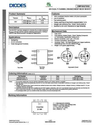
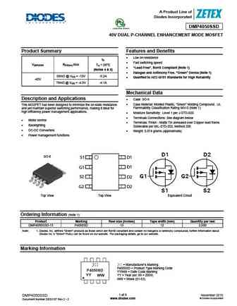
DMP4047SSD 40V DUAL P-CHANNEL ENHANCEMENT MODE MOSFET Product Summary Features 100% Unclamped Inductive Switch (UIS) test in production ID V(BR)DSS RDS(on) Low on-resistance TA = +25 C Fast switching speed 45m @ VGS = -10V -6.5A -40V Totally Lead-Free & Fully RoHS compliant (Note 1 & 2) 55m @ VGS = -4.5V -5.9A Halogen and Antimony Free. Gre... See More ⇒
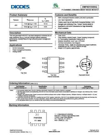
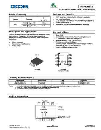
DMP4015SSSQ P-CHANNEL ENHANCEMENT MODE MOSFET Product Summary Features and Benefits 100% Unclamped Inductive Switch (UIS) test in production ID V(BR)DSS RDS(on) max Low Input Capacitance TA = +25 C Totally Lead-Free & Fully RoHS Compliant (Notes 1 & 2) 11m @ VGS = -10V -10.1A Halogen and Antimony Free. Green Device (Note 3) -40V Qualified to ... See More ⇒
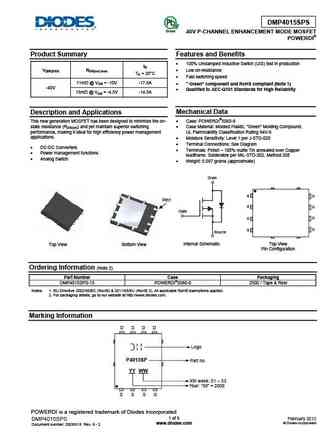
DMP4015SPS Green 40V P-CHANNEL ENHANCEMENT MODE MOSFET POWERDI Product Summary Features and Benefits 100% Unclamped Inductive Switch (UIS) test in production ID V(BR)DSS RDS(on) max Low on-resistance TA = 25 C Fast switching speed 11m @ VGS = -10V -17.0A " Green component and RoHS compliant (Note 1) -40V Qualified to AEC-Q101 Standards for Hig... See More ⇒
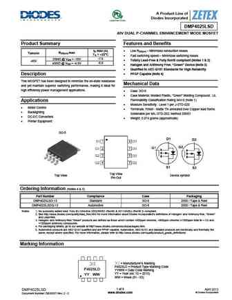
A Product Line of Diodes Incorporated DMP4025LSD 40V DUAL P-CHANNEL ENHANCEMENT MODE MOSFET Product Summary Features and Benefits ID max (A) Low RDS(on) Minimizes conduction losses V(BR)DSS RDS(on) max TA = +25 C Fast switching speed Minimizes switching losses 25m @ VGS = -10V -7.6 Totally Lead-Free & Fully RoHS compliant (Notes 1 & 2) -40V 45m @... See More ⇒
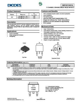
DMP4015SK3 P-CHANNEL ENHANCEMENT MODE MOSFET Product Summary Features and Benefits 100% Unclamped Inductive Switch (UIS) test in production ID V(BR)DSS RDS(on) max Low on-resistance TA = 25 C Fast switching speed 11m @ VGS = -10V -14.0A Green component and RoHS compliant (Note 1) -40V Qualified to AEC-Q101 Standards for High Reliability 15m ... See More ⇒
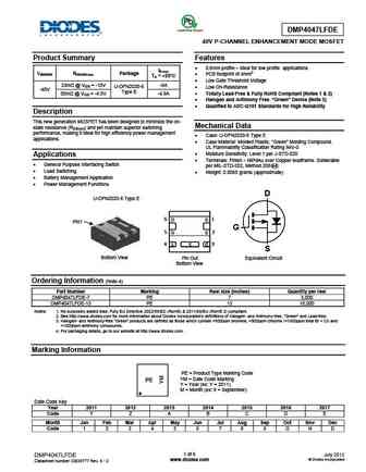
DMP4047LFDE 40V P-CHANNEL ENHANCEMENT MODE MOSFET Product Summary Features 0.6mm profile ideal for low profile applications ID max V(BR)DSS RDS(ON) max Package PCB footprint of 4mm2 TA = +25 C Low Gate Threshold Voltage 33m @ VGS = -10V -6A U-DFN2020-6 Low On-Resistance -40V Type E 50m @ VGS = -4.5V -4.9A Totally Lead-Free & Fully RoHS Com... See More ⇒
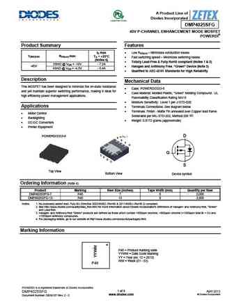
A Product Line of Diodes Incorporated DMP4025SFG 40V P-CHANNEL ENHANCEMENT MODE MOSFET POWERDI Product Summary Features ID max Low RDS(on) Minimizes conduction losses V(BR)DSS RDS(on) max TA = +25 C Fast switching speed Minimizes switching losses (Notes 6) Totally Lead-Free & Fully RoHS compliant (Notes 1 & 2) 25m @ VGS = -10V - 7.2A -40V Hal... See More ⇒
DMP4013LFG 40V P-CHANNEL ENHANCEMENT MODE MOSFET POWERDI Product Summary Features and Benefits Low RDS(ON) ensures on state losses are minimized. ID max BVDSS RDS(ON) max Small form factor thermally efficient package enables higher TA = +25 C 13m @ VGS = -10V -10.3A density end products. -40V 18m @ VGS = -4.5V -8.8A Occupies 33% of the board area ... See More ⇒
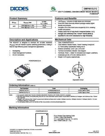
A Product Line of Diodes Incorporated Green DMP4051LK3 40V P-CHANNEL ENHANCEMENT MODE MOSFET Product Summary Features and Benefits Low on-resistance ID V(BR)DSS RDS(on) Fast switching speed TA = 25 C Green component and RoHS compliant (Note 1) 51m @ VGS= -10V -10.5A Qualified to AEC-Q101 Standards for High Reliability -40V 85m @ VGS= -4.5V -8.4... See More ⇒
A Product Line of Diodes Incorporated DMP4050SSD 40V DUAL P-CHANNEL ENHANCEMENT MODE MOSFET Product Summary Features and Benefits Low on-resistance ID Fast switching speed V(BR)DSS RDS(on) Max TA = 25 C Lead-Free , RoHS Compliant (Note 1) (Notes 4 & 6) Halogen and Antimony Free, Green Device (Note 1) 50m @ VGS = -10V -5.2A Qualified to ... See More ⇒
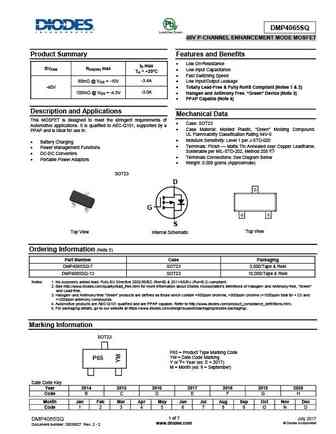
DMP4065SQ 40V P-CHANNEL ENHANCEMENT MODE MOSFET Product Summary Features and Benefits Low On-Resistance ID max BVDSS RDS(ON) max Low Input Capacitance TA = +25 C Fast Switching Speed -3.4A 80m @ VGS = -10V Low Input/Output Leakage -40V Totally Lead-Free & Fully RoHS Compliant (Notes 1 & 2) 100m @ VGS = -4.5V -3.0A Halogen and Antimony F... See More ⇒
A Product Line of Diodes Incorporated DMP4025LSS 40V P-CHANNEL ENHANCEMENT MODE MOSFET Product Summary Features and Benefits Low RDS(on) Minimizes conduction losses ID max (A) Fast switching speed Minimizes switching losses V(BR)DSS RDS(on) max TA = 25 C Totally Lead-Free & Fully RoHS compliant (Notes 1 & 2) (Notes 6) Halogen and Antimony Free. Gr... See More ⇒
DMP4013LFGQ 40V P-CHANNEL ENHANCEMENT MODE MOSFET PowerDI3333-8 Product Summary Features and Benefits Low RDS(ON) Ensures On-State Losses are Minimized ID Max BVDSS RDS(ON) Max Small Form Factor Thermally Efficient Package Enables Higher TA = +25 C 13m @ VGS = -10V -10.3A Density End Products -40V 18m @ VGS = -4.5V -8.8A Occupies 33% of the Board... See More ⇒
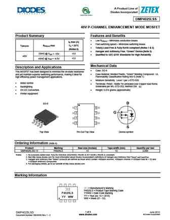
DMP4015SSS P-CHANNEL ENHANCEMENT MODE MOSFET Product Summary Features and Benefits 100% Unclamped Inductive Switch (UIS) test in production ID V(BR)DSS RDS(on) max Low Input Capacitance TA = 25 C Lead, Halogen, and Antimony Free, RoHS Compliant (Note 1) "Green" Device (Note 2) 11m @ VGS = -10V -10.1A -40V Qualified to AEC-Q101 Standards for High Rel... See More ⇒
DMP4025LK3 40V P-CHANNEL ENHANCEMENT MODE MOSFET Product Summary Features Low On-Resistance ID max BVDSS RDS(on) max TA = +25 C Fast Switching Speed (Note 6) Low Input/Output Leakage 25m @ VGS = -10V -8.6A Lead-Free Finish; RoHS compliant (Note 1 & 2) -40V 45m @ VGS = -4.5V -7.0A Halogen and Antimony Free. Green Device (Note 3) Quali... See More ⇒
DMP4047SK3 40V P-CHANNEL ENHANCEMENT MODE MOSFET Product Summary Features 100% Unclamped Inductive Switch (UIS) Test in Production ID V(BR)DSS RDS(ON) Low On-resistance TC = +25 C Fast Switching Speed Totally Lead-Free & Fully RoHS compliant (Notes 1 & 2) 45m @ VGS = -10V -20A -40V Halogen and Antimony Free. Green Device (Note 3) 55m @ VG... See More ⇒
A Product Line of Diodes Incorporated DMP4050SSS 40V P-CHANNEL ENHANCEMENT MODE MOSFET Product Summary Features and Benefits Low on-resistance ID V(BR)DSS RDS(on) Fast switching speed TA = 25 C Green component and RoHS compliant (Note 1) 50m @ VGS= -10V -6.0A Qualified to AEC-Q101 Standards for High Reliability -40V 79m @ VGS= -4.5V -4.7A Me... See More ⇒
DMP4065S 40V P-CHANNEL ENHANCEMENT MODE MOSFET Product Summary Features and Benefits Low On-Resistance ID max V(BR)DSS RDS(ON) max TA = 25 C Low Input Capacitance Fast Switching Speed -3.4A 80m @ VGS = -10V Low Input/Output Leakage -40V 100m @ VGS = -4.5V -3.0A Totally Lead-Free & Fully RoHS Compliant (Notes 1 & 2) Halogen and Antimon... See More ⇒
DMP4015SSSQ www.VBsemi.tw P-Channel 40 V (D-S) MOSFET FEATURES PRODUCT SUMMARY Halogen-free According to IEC 61249-2-21 VDS (V) RDS(on) ( )ID (A)a Qg (Typ.) Definition 0.010 at VGS = - 10 V - 16.1 100 % Rg Tested - 40 33 nC 0.014 at VGS = - 4.5 V - 13.3 100 % UIS Tested Compliant to RoHS Directive 2002/95/EC APPLICATIONS S Load Switch POL SO-8 G SD ... See More ⇒
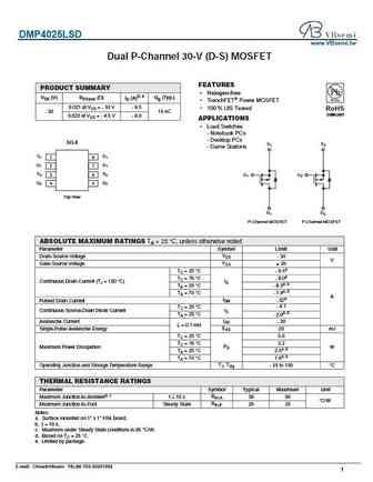
DMP4025LSD www.VBsemi.tw Dual P-Channel 30-V (D-S) MOSFET FEATURES PRODUCT SUMMARY Halogen-free VDS (V) RDS(on) ( ) ID (A)d, e Qg (Typ.) TrenchFET Power MOSFET 0.021 at VGS = - 10 V - 9.5 100 % UIS Tested RoHS - 30 15 nC COMPLIANT 0.028 at VGS = - 4.5 V - 8.0 APPLICATIONS Load Switches - Notebook PCs - Desktop PCs SO-8 S1 S2 - Game Stations S1 1 D1 8 ... See More ⇒
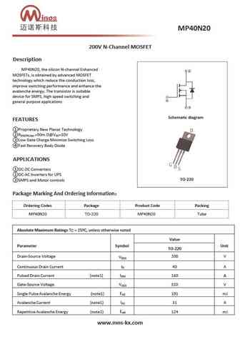
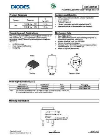
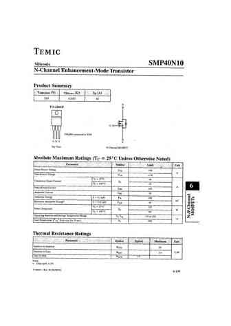
200V N-Channel MOSFET Description MP40N20, the silicon N-channel Enhanced MOSFETs, is obtained by advanced MOSFET technology which reduce the conduction loss, improve switching performance and enhance the avalanche energy. The transistor is suitable device for SMPS, high speed switching and general purpose applications Schematic diagram FEATURES Proprietary New Planar Technology ... See More ⇒

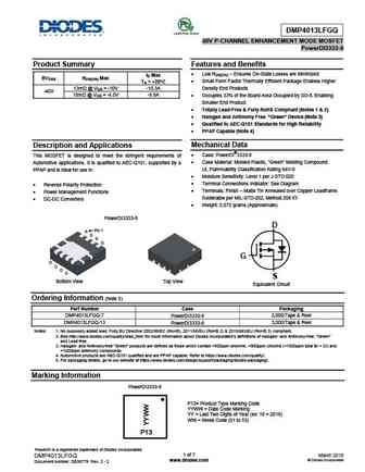
isc P-Channel MOSFET Transistor DMP4015SK3 FEATURES Drain Current I = -35A@ T =25 D C Drain Source Voltage- V = -40V(Min) DSS Static Drain-Source On-Resistance R = 11m (Max) DS(on) 100% avalanche tested Minimum Lot-to-Lot variations for robust device performance and reliable operation DESCRIPTION Designed for use in switch mode power supplies and general pu... See More ⇒
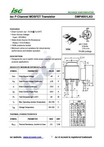
isc P-Channel MOSFET Transistor DMP4051LK3 FEATURES Drain Current I = -10.5A@ T =25 D C Drain Source Voltage- V = -40V(Min) DSS Static Drain-Source On-Resistance R = 51m (Max) DS(on) 100% avalanche tested Minimum Lot-to-Lot variations for robust device performance and reliable operation DESCRIPTION Designed for use in switch mode power supplies and general ... See More ⇒
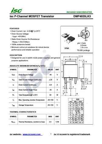
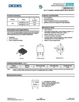
isc P-Channel MOSFET Transistor DMP4025LK3 FEATURES Drain Current I = -8.6A@ T =25 D C Drain Source Voltage- V = -40V(Min) DSS Static Drain-Source On-Resistance R = 25m (Max) DS(on) 100% avalanche tested Minimum Lot-to-Lot variations for robust device performance and reliable operation DESCRIPTION Designed for use in switch mode power supplies and general p... See More ⇒
Detailed specifications: MP3904, MP3904R, MP3905, MP3905R, MP3906, MP3906R, MP3962, MP39B, S8050, MP4048, MP4049, MP4050, MP4051, MP4052, MP4053, MP40A, MP41
Keywords - MP40 pdf specs
MP40 cross reference
MP40 equivalent finder
MP40 pdf lookup
MP40 substitution
MP40 replacement
