ST9 Specs and Replacement
Type Designator: ST9
Material of Transistor: Si
Polarity: NPN
Absolute Maximum Ratings
Maximum Collector Power Dissipation (Pc): 0.15 W
Maximum Collector-Emitter Voltage |Vce|: 15 V
Maximum Collector Current |Ic max|: 0.05 A
Max. Operating Junction Temperature (Tj): 175 °C
Electrical Characteristics
Transition Frequency (ft): 20 MHz
Collector Capacitance (Cc): 3 pF
Forward Current Transfer Ratio (hFE), MIN: 30
Noise Figure, dB: -
Package: TO5
- BJT ⓘ Cross-Reference Search
ST9 datasheet
0.1. Size:250K st
std901t st901t.pdf 

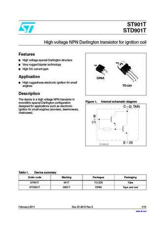
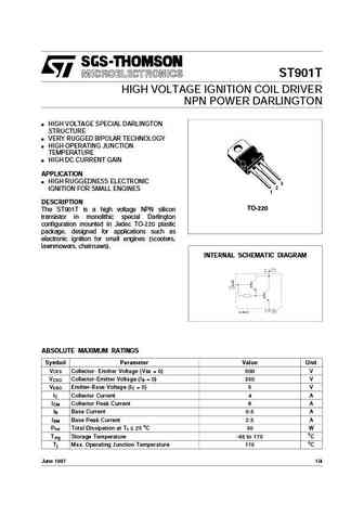
ST901T STD901T High voltage NPN Darlington transistor for ignition coil Features High voltage special Darlington structure TAB Very rugged bipolar technology TAB High DC current gain 3 1 Application 3 DPAK 2 1 High ruggedness electronic ignition for small TO-220 engines Description The device is a high voltage NPN transistor in Figure 1. Internal schematic... See More ⇒
0.2. Size:282K st
st93003.pdf 

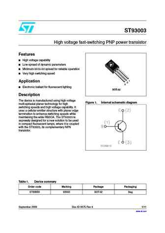
ST93003 High voltage fast-switching PNP power transistor Features High voltage capability Low spread of dynamic parameters Minimum lot-to-lot spread for reliable operation Very high switching speed 1 Application 2 3 Electronic ballast for fluorescent lighting SOT-32 Description The device is manufactured using high voltage Figure 1. Internal schematic diagram... See More ⇒
0.3. Size:110K fairchild semi
kst92 kst93.pdf 

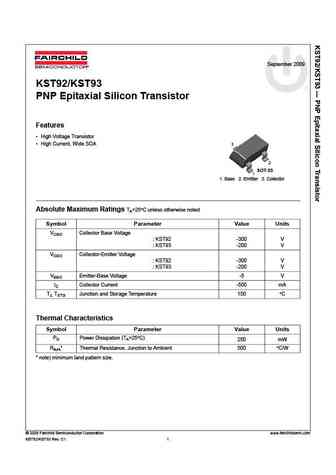
September 2009 KST92/KST93 PNP Epitaxial Silicon Transistor Features High Voltage Transistor High Current, Wide SOA 3 2 SOT-23 1 1. Base 2. Emitter 3. Collector Absolute Maximum Ratings TA=25 C unless otherwise noted Symbol Parameter Value Units VCBO Collector Base Voltage KST92 -300 V KST93 -200 V VCEO Collector-Emitter Voltage KST92 -300 V KST93 -200 V ... See More ⇒
0.4. Size:46K fairchild semi
kst92.pdf 

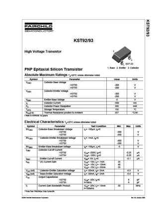
KST92/93 3 High Voltage Transistor 2 SOT-23 1 1. Base 2. Emitter 3. Collector PNP Epitaxial Silicon Transistor Absolute Maximum Ratings Ta=25 C unless otherwise noted Symbol Parameter Value Units VCBO Collector Base Voltage KST92 -300 V KST93 -200 V VCEO Collector-Emitter Voltage KST92 -300 V KST93 -200 V VEBO Emitter-Base Voltage -5 V IC Collector Current -500 mA... See More ⇒
0.5. Size:21K samsung
kst92.pdf 

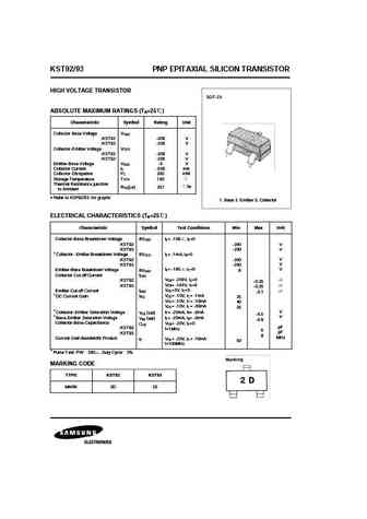
KST92/93 PNP EPITAXIAL SILICON TRANSISTOR HIGH VOLTAGE TRANSISTOR SOT-23 ABSOLUTE MAXIMUM RATINGS (T =25 ) A Characteristic Symbol Rating Unit Collector Base Voltage VCBO KST92 -300 V KST93 -200 V Collector-Emitter Voltage VCEO KST92 -300 V KST93 -200 V Emitter-Base Voltage VEBO -5 V Collector Current IC -500 mA Collector Dissipation PC 350 mW Storage Temperature TSTG 15... See More ⇒
0.6. Size:63K rohm
qst9.pdf 

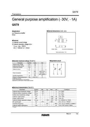
QST9 Transistors General purpose amplification (-30V, -1A) QST9 External dimensions (Unit mm) Application Low frequency amplifier Driver 2.8 1.6 Features 1) Collector current is large. 2) Collector saturation voltage is low. VCE(sat) max. -350mV At IC = -500mA / IB = -25mA ROHM TSMT6 Each lead has same dimensions Abbreviated symbol T09 Equivalent circui... See More ⇒
0.7. Size:515K kexin
kst9018.pdf 

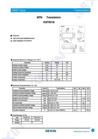
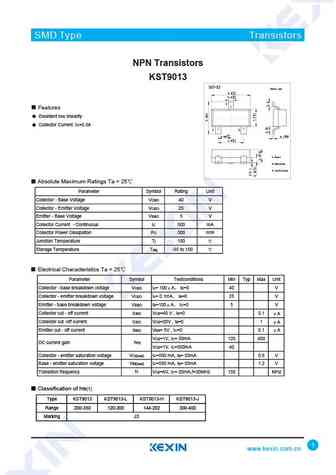
SMD Type SMD Type Tra n s i s to rs IC SMD Type NPN Transistors KST9018 SOT-23 Unit mm +0.1 2.9-0.1 +0.1 0.4 -0.1 3 Features Features High current gain bandwidth product. 1 2 +0.1 +0.05 power dissipation.(PC=200mW) 0.95 -0.1 0.1 -0.01 1.9+0.1 -0.1 1.Base 2.Emitter 3.collector Absolute Maximum Ratings Ta = 25 Parameter Symbol Rating Unit Col... See More ⇒
0.8. Size:388K kexin
kst9013c.pdf 

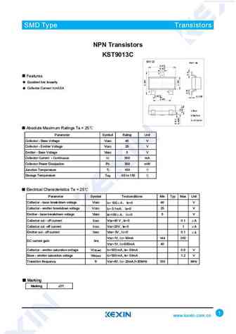
SMD Type IC SMD Type Transistors SMD Type NPN Transistors KST9013C SOT-23 Unit mm 2.9+0.1 -0.1 +0.1 0.4-0.1 3 Features Excellent hFE linearity Collector Current IC=0.5A 12 +0.1 +0.05 0.95-0.1 0.1 -0.01 +0.1 1.9 -0.1 1.Base 2.Emitter 3.collector Absolute Maximum Ratings Ta = 25 Parameter Symbol Rating Unit Collector - Base Voltage VCBO 40 V Collector - Emitter Voltag... See More ⇒
0.9. Size:1021K kexin
kst9014-d.pdf 

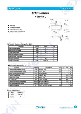
SMD Type Transistors SMD Type NPN Transistors KST9014-D SOT-23 Unit mm +0.1 2.9-0.1 +0.1 0.4 -0.1 3 Features Excellent hFE linearity Collector Current IC=0.1A 1 2 +0.05 0.95+0.1 -0.1 0.1 -0.01 Complementary to KST9015-D 1.9+0.1 -0.1 1.Base 2.Emitter 3.collector Absolute Maximum Ratings Ta = 25 Parameter Symbol Rating Unit Collector-Base Voltage VCBO 50 V Collector-E... See More ⇒
0.10. Size:1068K kexin
kst9015-d.pdf 

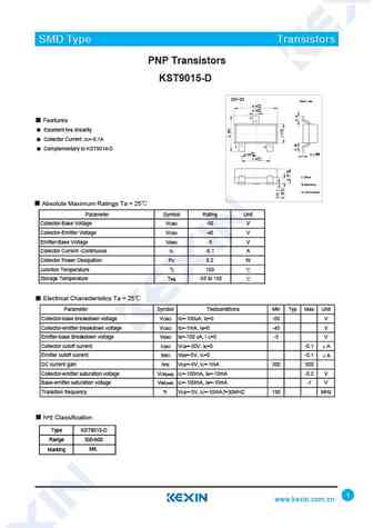
SMD Type Transistors SMD Type PNP Transistors KST9015-D SOT-23 Unit mm +0.1 2.9 -0.1 +0.1 0.4-0.1 3 Features Excellent hFE linearity Collector Current IC=-0.1A 1 2 Complementary to KST9014-D +0.1 +0.05 0.95 -0.1 0.1 -0.01 +0.1 1.9 -0.1 1.Base 2.Emitter 3.collector Absolute Maximum Ratings Ta = 25 Parameter Symbol Rating Unit Collector-Base Voltage VCBO -50 V Collect... See More ⇒
0.11. Size:925K kexin
kst9014.pdf 

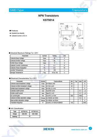
SMD Type Transistors SMD Type NPN Transistors KST9014 SOT-23 Unit mm +0.1 2.9-0.1 +0.1 0.4 -0.1 3 Features Excellent hFE linearity Collector Current IC=0.1A 1 2 +0.05 0.95+0.1 -0.1 0.1 -0.01 1.9+0.1 -0.1 1.Base 2.Emitter 3.collector Absolute Maximum Ratings Ta = 25 Parameter Symbol Rating Unit Collector-Base Voltage VCBO 50 V Collector-Emitter Voltage VCEO 45 V Emit... See More ⇒
0.12. Size:137K kexin
kst9012c.pdf 

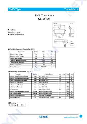
SMD Type Transistors SMD Type IC SMD Type PNP Transistors KST9012C SOT-23 Unit mm +0.1 2.9 -0.1 +0.1 0.4-0.1 3 Features Excellent hFE liearity Collector Current IC=-0.5A 12 +0.05 0.95+0.1 -0.1 0.1-0.01 +0.1 1.9 -0.1 1.Base 2.Emitter 3.collector Absolute Maximum Ratings Ta = 25 Parameter Symbol Rating Unit Collector - Base Voltage VCBO -40 V Collector - Emitter Voltag... See More ⇒
0.13. Size:987K kexin
kst9013.pdf 

SMD Type TransistICs SMD Type or SMD Type NPN Transistors KST9013 SOT-23 Unit mm +0.1 2.9-0.1 +0.1 0.4 -0.1 3 Features Excellent hFE linearity Collector Current IC=0.5A 1 2 +0.1 0.95-0.1 0.1+0.05 -0.01 1.9+0.1 -0.1 1.Base 2.Emitter 3.collector Absolute Maximum Ratings Ta = 25 Parameter Symbol Rating Unit Collector - Base Voltage VCBO 40 V Collector - Emitter Voltage... See More ⇒
0.14. Size:971K kexin
kst9015.pdf 

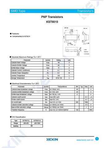
SMD Type Transistors SMD Type PNP Transistors KST9015 SOT-23 Unit mm +0.1 2.9 -0.1 +0.1 0.4-0.1 3 Features Complementary to KST9014 1 2 +0.1 +0.05 0.95 -0.1 0.1 -0.01 +0.1 1.9 -0.1 1.Base 2.Emitter 3.collector Absolute Maximum Ratings Ta = 25 Parameter Symbol Rating Unit Collector-Base Voltage VCBO -50 V Collector-Emitter Voltage VCEO -45 V Emitter-Base Voltage VEBO -... See More ⇒
0.15. Size:911K kexin
kst9012.pdf 

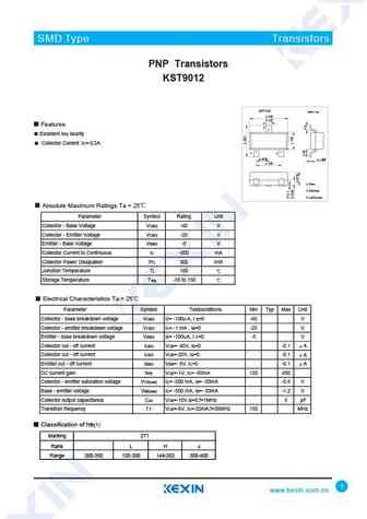
SMD Type or SMD Type TransistICs SMD Type PNP Transistors KST9012 SOT-23 Unit mm +0.1 2.9 -0.1 +0.1 0.4 -0.1 Features 3 Excellent hFE liearity Collector Current IC=-0.5A 1 2 +0.1 +0.05 0.95 -0.1 0.1 -0.01 +0.1 1.9 -0.1 1.Base 2.Emitter 3.collector Absolute Maximum Ratings Ta = 25 Parameter Symbol Rating Unit Collector - Base Voltage VCBO -40 V Collector - Emitter Vo... See More ⇒
0.16. Size:785K oriental semi
ost90n65hm2f.pdf 

OST90N65HM2F Enhancement Mode N-Channel Power IGBT General Description OST90N65HM2F uses advanced Oriental-Semi s patented Trident-Gate Bipolar Transistor (TGBTTM) technology to provide extremely low V (sat), low gate charge, and excellent switching CE performance. This device is suitable for mid to high range switching frequency converters. Features Advanced TGBTTM technol... See More ⇒
0.17. Size:481K oriental semi
ost90n60hczf.pdf 

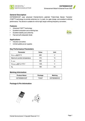
OST90N60HCZF Enhancement Mode N-Channel Power IGBT General Description OST90N60HCZF uses advanced Oriental-Semi s patented Trident-Gate Bipolar Transistor (TGBTTM) technology to provide extremely low V (sat), low gate charge, and excellent switching CE performance. This device is suitable for mid to high range switching frequency converters. Features Advanced TGBTTM technol... See More ⇒
0.18. Size:396K stansontech
st9435a.pdf 

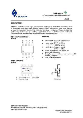
ST9435A P Channel Enhancement Mode MOSFET - 5.6A DESCRIPTION ST9435A is the P-Channel logic enhancement mode power field effect transistor which is produced using high cell density, DMOS trench technology. This high density process is especially tailored to minimize on-state resistance. These devices are particularly suited for low voltage application such as battery pack, note... See More ⇒
0.19. Size:60K stansontech
st901t.pdf 

ST901T HIGH VOLTAGE IGNITION COIL DRIVER NPN POWER DARLINGTON HIGH VOLTAGE SPECIAL DARLINGTON STRUCTURE VERY RUGGED BIPOLAR TECHNOLOGY HIGH OPERATING JUNCTION TEMPERATURE HIGH DC CURRENT GAIN APPLICATION HIGH RUGGEDNESS ELECTRONIC 3 2 IGNITION FOR SMALL ENGINES 1 DESCRIPTION TO-220 The ST901T is a high voltage NPN silicon transistor in monolithic special Darlington con... See More ⇒
0.20. Size:359K stansontech
st9435gp.pdf 

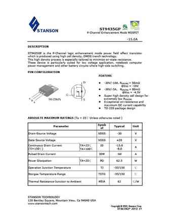
ST9435GP P Channel Enhancement Mode MOSFET -15.0A DESCRIPTION ST9435GP is the P-Channel logic enhancement mode power field effect transistor which is produced using high cell density, DMOS trench technology. This high density process is especially tailored to minimize on-state resistance. These device is particularly suited for low voltage application, notebook computer power... See More ⇒
0.21. Size:725K convert
cst9n20lf cst9n20lp.pdf 

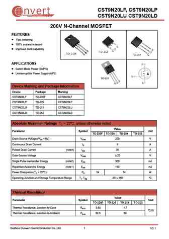
CST9N20LF, CST9N20LP nvert Suzhou Convert Semiconductor Co ., Ltd. CST9N20LU CST9N20LD 200V N-Channel MOSFET FEATURES Fast switching 100% avalanche tested Improved dv/dt capability APPLICATIONS Switch Mode Power (SMPS) Uninterruptible Power Supply (UPS) Device Marking and Package Information Device Package Marking CST9N20LF TO-220F CST9N20LF CST9N20LP TO-220 C... See More ⇒
0.22. Size:984K cn super semi
ssf90r420s2 ssp90r420s2 sst90r420s2.pdf 

SUPER-SEMI SUPER-MOSFET Super Junction Metal Oxide Semiconductor Field Effect Transistor 900V Super Junction Power MOSFET Gen- SS*90R420S2 Rev. 1.2 Nov. 2022 www.supersemi.com.cn SSF90R420S2/SSP90R420S2/SST90R420S2 900V N-Channel Super-Junction MOSFET Gen- Description Features SJ-FET is new generation of high voltage MOSFET family that Multi-Epi process SJ-FET is utilizin... See More ⇒
0.23. Size:993K cn super semi
ssf90r900s2 ssp90r900s2 sst90r900s2.pdf 

SUPER-SEMI SUPER-MOSFET Super Junction Metal Oxide Semiconductor Field Effect Transistor 900V Super Junction Power MOSFET Gen- SS*90R900S2 Rev. 1.2 May. 2022 www.supersemi.com.cn SSF90R900S2/SSP90R900S2/SST90R900S2 900V N-Channel Super-Junction MOSFET Gen- Description Features SJ-FET is new generation of high voltage MOSFET family that Multi-Epi process SJ-FET is utilizin... See More ⇒
0.24. Size:890K cn super semi
ssf90r650s2 ssp90r650s2 sst90r650s2.pdf 

SUPER-SEMI SUPER-MOSFET Super Junction Metal Oxide Semiconductor Field Effect Transistor 900V Super Junction Power MOSFET Gen- SS*90R650S2 Rev. 1.2 Jul. 2022 www.supersemi.com.cn SSF90R650S2/SSP90R650S2/SST90R650S2 900V N-Channel Super-Junction MOSFET Gen- Description Features SJ-FET is new generation of high voltage MOSFET family that Multi-Epi process SJ-FET is utilizin... See More ⇒
0.25. Size:1120K cn super semi
ssf90r1k5s ssp90r1k5s sst90r1k5s ssu90r1k5s.pdf 

SUPER-SEMI SUPER-MOSFET Super Junction Metal Oxide Semiconductor Field Effect Transistor 900V Super Junction Power MOSFET SS*90R1K5S Rev. 1.2 Aug. 2019 www.supersemi.com.cn September, 2013 SJ-FET SSF90R1K5S/SSP90R1K5S/SST90R1K5S/SSU90R1K5S 900V N-Channel MOSFET Description Features SJ-FET is new generation of high voltage MOSFET family that Multi-Epi process SJ-FET is utilizi... See More ⇒
Detailed specifications: ST6008, ST6010, ST61, ST63, ST8033, ST8035, ST8065, ST8509, A1013, ST905, STC1725, STC1727, STC1729, STC1730, STC1732, STC1734, STC1735
Keywords - ST9 pdf specs
ST9 cross reference
ST9 equivalent finder
ST9 pdf lookup
ST9 substitution
ST9 replacement
