TK31 Specs and Replacement
Type Designator: TK31
Material of Transistor: Ge
Polarity: PNP
Absolute Maximum Ratings
Maximum Collector Power Dissipation (Pc): 0.2
W
Maximum Collector-Base Voltage |Vcb|: 20
V
Maximum Collector-Emitter Voltage |Vce|: 5
V
Maximum Emitter-Base Voltage |Veb|: 15
V
Maximum Collector Current |Ic max|: 0.1
A
Max. Operating Junction Temperature (Tj): 75
°C
Electrical Characteristics
Transition Frequency (ft): 6
MHz
Forward Current Transfer Ratio (hFE), MIN: 20
Noise Figure, dB: -
Package: X18
-
BJT ⓘ Cross-Reference Search
TK31 datasheet
0.1. Size:241K toshiba
tk31v60w.pdf 
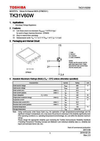
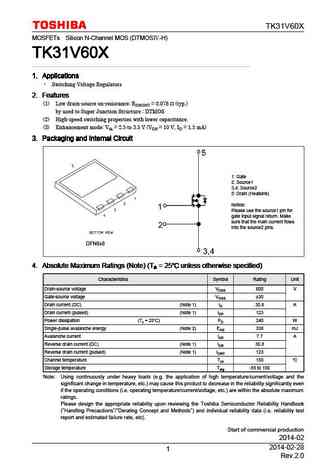
TK31V60W MOSFETs Silicon N-Channel MOS (DTMOS ) TK31V60W TK31V60W TK31V60W TK31V60W 1. Applications 1. Applications 1. Applications 1. Applications Switching Voltage Regulators 2. Features 2. Features 2. Features 2. Features (1) Low drain-source on-resistance RDS(ON) = 0.078 (typ.) by used to Super Junction Structure DTMOS (2) Easy to control Gate switching (3) E... See More ⇒
0.2. Size:250K toshiba
tk31a60w.pdf
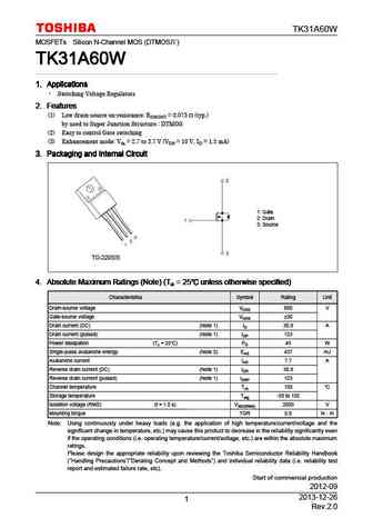
TK31A60W MOSFETs Silicon N-Channel MOS (DTMOS ) TK31A60W TK31A60W TK31A60W TK31A60W 1. Applications 1. Applications 1. Applications 1. Applications Switching Voltage Regulators 2. Features 2. Features 2. Features 2. Features (1) Low drain-source on-resistance RDS(ON) = 0.073 (typ.) by used to Super Junction Structure DTMOS (2) Easy to control Gate switching (3) E... See More ⇒
0.3. Size:249K toshiba
tk31n60x.pdf

TK31N60X MOSFETs Silicon N-Channel MOS (DTMOS -H) TK31N60X TK31N60X TK31N60X TK31N60X 1. Applications 1. Applications 1. Applications 1. Applications Switching Voltage Regulators 2. Features 2. Features 2. Features 2. Features (1) Low drain-source on-resistance RDS(ON) = 0.073 (typ.) by used to Super Junction Structure DTMOS (2) High-speed switching properties wit... See More ⇒
0.4. Size:274K toshiba
tk31v60w5.pdf
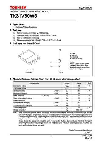
TK31V60W5 MOSFETs Silicon N-Channel MOS (DTMOS ) TK31V60W5 TK31V60W5 TK31V60W5 TK31V60W5 1. Applications 1. Applications 1. Applications 1. Applications Switching Voltage Regulators 2. Features 2. Features 2. Features 2. Features (1) Fast reverse recovery time trr = 135 ns (typ.) (2) Low drain-source on-resistance RDS(ON) = 0.087 (typ.) (3) Easy to control Gate switc... See More ⇒
0.5. Size:243K toshiba
tk31j60w5.pdf

TK31J60W5 MOSFETs Silicon N-Channel MOS (DTMOS ) TK31J60W5 TK31J60W5 TK31J60W5 TK31J60W5 1. Applications 1. Applications 1. Applications 1. Applications Switching Voltage Regulators 2. Features 2. Features 2. Features 2. Features (1) Fast reverse recovery time trr = 135 ns (typ.) (2) Low drain-source on-resistance RDS(ON) = 0.082 (typ.) by using Super Junction Stru... See More ⇒
0.6. Size:244K toshiba
tk31n60w5.pdf
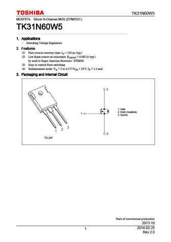
TK31N60W5 MOSFETs Silicon N-Channel MOS (DTMOS ) TK31N60W5 TK31N60W5 TK31N60W5 TK31N60W5 1. Applications 1. Applications 1. Applications 1. Applications Switching Voltage Regulators 2. Features 2. Features 2. Features 2. Features (1) Fast reverse recovery time trr = 135 ns (typ.) (2) Low drain-source on-resistance RDS(ON) = 0.082 (typ.) by used to Super Junction St... See More ⇒
0.7. Size:241K toshiba
tk31v60x.pdf
TK31V60X MOSFETs Silicon N-Channel MOS (DTMOS -H) TK31V60X TK31V60X TK31V60X TK31V60X 1. Applications 1. Applications 1. Applications 1. Applications Switching Voltage Regulators 2. Features 2. Features 2. Features 2. Features (1) Low drain-source on-resistance RDS(ON) = 0.078 (typ.) by used to Super Junction Structure DTMOS (2) High-speed switching properties wit... See More ⇒
0.8. Size:258K toshiba
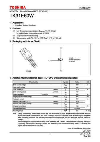
tk31e60w.pdf
TK31E60W MOSFETs Silicon N-Channel MOS (DTMOS ) TK31E60W TK31E60W TK31E60W TK31E60W 1. Applications 1. Applications 1. Applications 1. Applications Switching Voltage Regulators 2. Features 2. Features 2. Features 2. Features (1) Low drain-source on-resistance RDS(ON) = 0.073 (typ.) by used to Super Junction Structure DTMOS (2) Easy to control Gate switching (3) E... See More ⇒
0.9. Size:251K toshiba
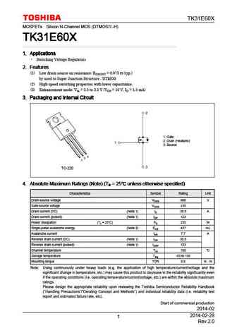
tk31e60x.pdf
TK31E60X MOSFETs Silicon N-Channel MOS (DTMOS -H) TK31E60X TK31E60X TK31E60X TK31E60X 1. Applications 1. Applications 1. Applications 1. Applications Switching Voltage Regulators 2. Features 2. Features 2. Features 2. Features (1) Low drain-source on-resistance RDS(ON) = 0.073 (typ.) by used to Super Junction Structure DTMOS (2) High-speed switching properties wit... See More ⇒
0.10. Size:255K toshiba
tk31n60w.pdf

TK31N60W MOSFETs Silicon N-Channel MOS (DTMOS ) TK31N60W TK31N60W TK31N60W TK31N60W 1. Applications 1. Applications 1. Applications 1. Applications Switching Voltage Regulators 2. Features 2. Features 2. Features 2. Features (1) Low drain-source on-resistance RDS(ON) = 0.073 (typ.) by used to Super Junction Structure DTMOS (2) Easy to control Gate switching (3) E... See More ⇒
0.11. Size:251K toshiba
tk31j60w.pdf

TK31J60W MOSFETs Silicon N-Channel MOS (DTMOS ) TK31J60W TK31J60W TK31J60W TK31J60W 1. Applications 1. Applications 1. Applications 1. Applications Switching Voltage Regulators 2. Features 2. Features 2. Features 2. Features (1) Low drain-source on-resistance RDS(ON) = 0.073 (typ.) by used to Super Junction Structure DTMOS (2) Easy to control Gate switching (3) E... See More ⇒
0.12. Size:125K onsemi
ntk3142p.pdf

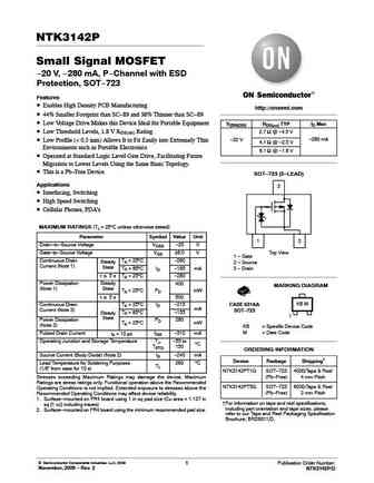
NTK3142P Small Signal MOSFET -20 V, -280 mA, P-Channel with ESD Protection, SOT-723 Features Enables High Density PCB Manufacturing http //onsemi.com 44% Smaller Footprint than SC-89 and 38% Thinner than SC-89 Low Voltage Drive Makes this Device Ideal for Portable Equipment V(BR)DSS RDS(on) TYP ID Max Low Threshold Levels, 1.8 V RDS(on) Rating 2.7 W @ -4.5 V -280 mA ... See More ⇒
0.13. Size:122K onsemi
ntk3142pt1g.pdf
NTK3142P Small Signal MOSFET -20 V, -280 mA, P-Channel with ESD Protection, SOT-723 Features Enables High Density PCB Manufacturing http //onsemi.com 44% Smaller Footprint than SC-89 and 38% Thinner than SC-89 Low Voltage Drive Makes this Device Ideal for Portable Equipment V(BR)DSS RDS(on) TYP ID Max Low Threshold Levels, 1.8 V RDS(on) Rating 2.7 W @ -4.5 V -280 mA ... See More ⇒
0.15. Size:61K onsemi
ntk3134n.pdf
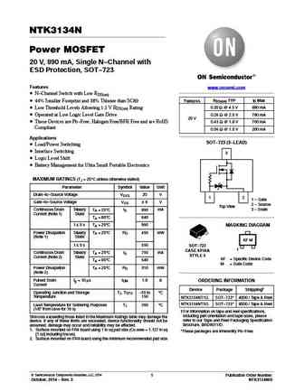
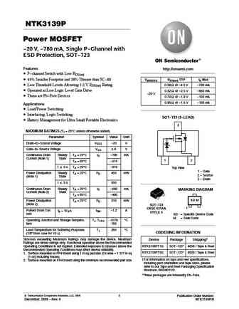
NTK3134N Power MOSFET 20 V, 890 mA, Single N-Channel with ESD Protection, SOT-723 Features www.onsemi.com N-Channel Switch with Low RDS(on) V(BR)DSS RDS(on) TYP ID Max 44% Smaller Footprint and 38% Thinner than SC89 0.20 W @ 4.5 V 890 mA Low Threshold Levels Allowing 1.5 V RDS(on) Rating Operated at Low Logic Level Gate Drive 0.26 W @ 2.5 V 790 mA 20 V These Dev... See More ⇒
0.16. Size:129K onsemi
ntk3139p.pdf
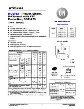
NTK3139P MOSFET Power, Single, P-Channel with ESD Protection, SOT-723 -20 V, -780 mA www.onsemi.com Features V(BR)DSS RDS(on) TYP ID Max P-channel Switch with Low RDS(on) 0.38 W @ -4.5 V -780 mA 44% Smaller Footprint and 38% Thinner than SC-89 0.52 W @ -2.5 V -660 mA Low Threshold Levels Allowing 1.5 V RDS(on) Rating -20 V 0.70 W @ -1.8 V -100 mA Operated at ... See More ⇒
0.17. Size:58K onsemi
ntk3134n-d ntk3134nt1g.pdf
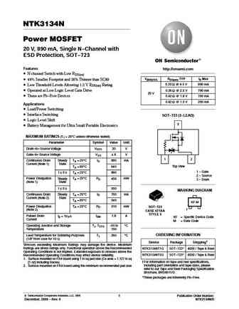
NTK3134N Power MOSFET 20 V, 890 mA, Single N-Channel with ESD Protection, SOT-723 Features http //onsemi.com N channel Switch with Low RDS(on) V(BR)DSS RDS(on) TYP ID Max 44% Smaller Footprint and 38% Thinner than SC89 0.20 W @ 4.5 V 890 mA Low Threshold Levels Allowing 1.5 V RDS(on) Rating Operated at Low Logic Level Gate Drive 0.26 W @ 2.5 V 790 mA 20 V These ... See More ⇒
0.18. Size:371K first silicon
ftk3139k.pdf
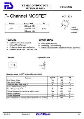
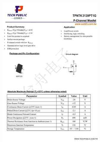
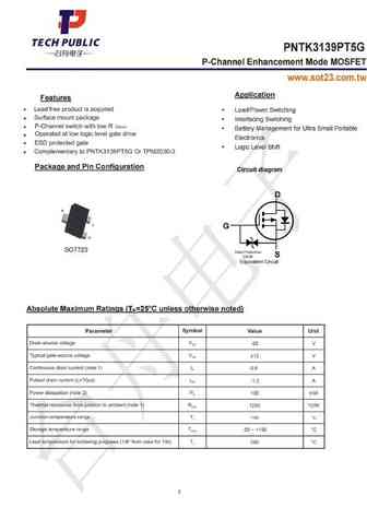
SEMICONDUCTOR FTK3139K TECHNICAL DATA SOT-723 P-Channel MOSFET ID V(BR)DSS RDS(on) MAX 520m @-4.5V 1. GATE 700m @-2.5V -20V -0.66A 2. SOURCE 950m @-1.8V 3. DRAIN FEATURE APPLICATION Lead Free Product is Acquired Load/Power Switching Surface Mount Package Interfacing, Logic Switching P-Channel Switch with Low RDS (on) Battery Management for Ultra... See More ⇒
0.19. Size:336K first silicon
ftk3134k.pdf
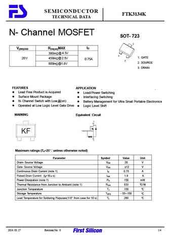
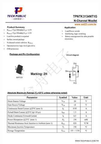
SEMICONDUCTOR FTK3134K TECHNICAL DATA N-Channel MOSFET SOT-723 ID V(BR)DSS RDS(on)MAX 380m @ 4.5V 1. GATE 20V 450m @ 2.5V 0.75A 2. SOURCE 800m @1.8V 3. DRAIN FEATURES APPLICATION Lead Free Product is Acquired Load/Power Switching Surface Mount Package Interfacing Switching N-Channel Switch with Low R(on) DS Battery Management for Ultra Small Portabl... See More ⇒
0.20. Size:398K first silicon
ftk3134kd.pdf
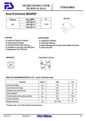
SEMICONDUCTOR FTK3134KD TECHNICAL DATA Dual N-Channel MOSFET SOT-363 ID V(BR)DSS RDS(on)MAX 380m @ 4.5V 0.75A 450m @ 2.5V 20V 800m @1.8V FEATURE APPLICATION Lead Free Product is Acquired Load/Power Switching Surface Mount Package Interfacing Switching N-Channel Switch with Low RDS(on) Battery Management for Ultra Small Portable Electronics... See More ⇒
0.24. Size:253K inchange semiconductor
tk31a60w.pdf
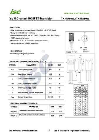
INCHANGE Semiconductor Isc N-Channel MOSFET Transistor TK31A60W, ITK31A60W FEATURES Low drain-source on-resistance RDS(ON) = 0.073 (typ.) Easy to control Gate switching Enhancement mode Vth = 2.7 to 3.7V (VDS = 10 V, ID=1.5mA) 100% avalanche tested Minimum Lot-to-Lot variations for robust device performance and reliable operation DESCRITION Switching Voltage Regul... See More ⇒
0.25. Size:246K inchange semiconductor
tk31e60w.pdf
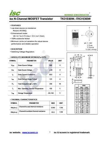
INCHANGE Semiconductor isc N-Channel MOSFET Transistor TK31E60W ITK31E60W FEATURES Low drain-source on-resistance RDS(on) 0.088 . Enhancement mode Vth =2.7 to 3.7V (VDS = 10 V, ID=1.5mA) 100% avalanche tested Minimum Lot-to-Lot variations for robust device performance and reliable operation DESCRITION Switching Voltage Regulators ABSOLUTE MAXIMUM RATINGS(T... See More ⇒
0.26. Size:213K inchange semiconductor
tk31n60w.pdf
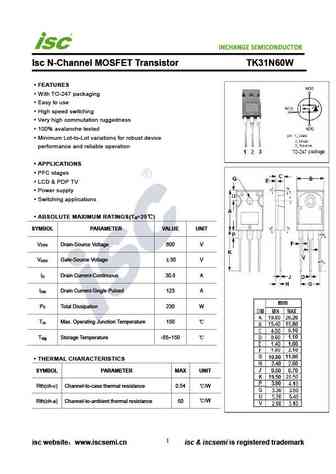
INCHANGE Semiconductor Isc N-Channel MOSFET Transistor TK31N60W FEATURES With TO-247 packaging Easy to use High speed switching Very high commutation ruggedness 100% avalanche tested Minimum Lot-to-Lot variations for robust device performance and reliable operation APPLICATIONS PFC stages LCD & PDP TV Power supply Switching applications ABSOLUTE MAXIMUM ... See More ⇒
Detailed specifications: TK259A
, TK25B
, TK25C
, TK264A
, TK28
, TK28C
, TK30
, TK30D
, A1015
, TK31D
, TK33
, TK33C
, TK34
, TK34C
, TK35
, TK35C
, TK36
.
History: 2SD1267A
| TIX618
Keywords - TK31 pdf specs
TK31 cross reference
TK31 equivalent finder
TK31 pdf lookup
TK31 substitution
TK31 replacement