TK33 Datasheet. Specs and Replacement
Type Designator: TK33 📄📄
Material of Transistor: Ge
Polarity: NPN
Absolute Maximum Ratings
Maximum Collector Power Dissipation (Pc): 0.1 W
Maximum Collector-Base Voltage |Vcb|: 30 V
Maximum Collector-Emitter Voltage |Vce|: 12 V
Maximum Emitter-Base Voltage |Veb|: 20 V
Maximum Collector Current |Ic max|: 0.05 A
Max. Operating Junction Temperature (Tj): 75 °C
Electrical Characteristics
Transition Frequency (ft): 3 MHz
Forward Current Transfer Ratio (hFE), MIN: 20
Package: X18
TK33 Substitution
- BJT ⓘ Cross-Reference Search
TK33 datasheet
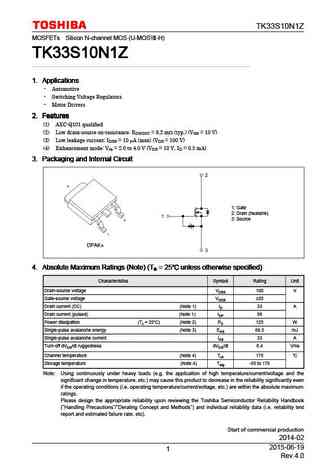
TK33S10N1Z MOSFETs Silicon N-channel MOS (U-MOS -H) TK33S10N1Z TK33S10N1Z TK33S10N1Z TK33S10N1Z 1. Applications 1. Applications 1. Applications 1. Applications Automotive Switching Voltage Regulators Motor Drivers 2. Features 2. Features 2. Features 2. Features (1) AEC-Q101 qualified (2) Low drain-source on-resistance RDS(ON) = 8.2 m (typ.) (VGS = 10 V) (3) ... See More ⇒
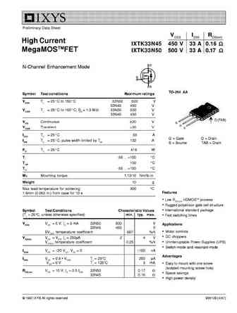
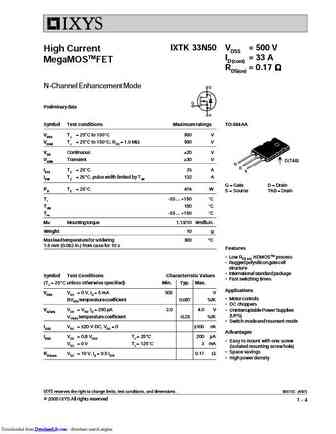
IXTK 33N50 VDSS = 500 V High Current ID (cont) = 33 A MegaMOSTMFET RDS(on) = 0.17 N-Channel Enhancement Mode Preliminary data Symbol Test conditions Maximum ratings TO-264 AA VDSS TJ = 25 C to 150 C 500 V VDGR TJ = 25 C to 150 C; RGS = 1.0 M 500 V VGS Continuous 20 V VGSM Transient 30 V D (TAB) G D ID25 TC = 25 C 33 A S IDM TC = 25 C, pulse ... See More ⇒
Detailed specifications: TK25C, TK264A, TK28, TK28C, TK30, TK30D, TK31, TK31D, BD140, TK33C, TK34, TK34C, TK35, TK35C, TK36, TK36C, TK37
Keywords - TK33 pdf specs
TK33 cross reference
TK33 equivalent finder
TK33 pdf lookup
TK33 substitution
TK33 replacement


