TP3053 Datasheet. Specs and Replacement
Type Designator: TP3053 📄📄
Material of Transistor: Si
Polarity: NPN
Absolute Maximum Ratings
Maximum Collector Power Dissipation (Pc): 1 W
Maximum Collector-Base Voltage |Vcb|: 60 V
Maximum Collector-Emitter Voltage |Vce|: 40 V
Maximum Emitter-Base Voltage |Veb|: 5 V
Maximum Collector Current |Ic max|: 0.7 A
Max. Operating Junction Temperature (Tj): 150 °C
Electrical Characteristics
Transition Frequency (ft): 100 MHz
Collector Capacitance (Cc): 15 pF
Forward Current Transfer Ratio (hFE), MIN: 50
Package: TO92
TP3053 Substitution
- BJT ⓘ Cross-Reference Search
TP3053 datasheet
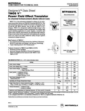
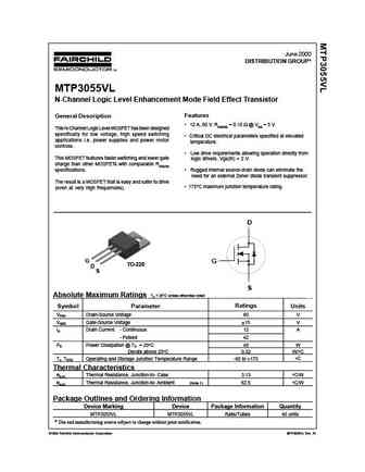
MOTOROLA Order this document SEMICONDUCTOR TECHNICAL DATA by MTP3055VL/D Designer's Data Sheet MTP3055VL TMOS V Motorola Preferred Device Power Field Effect Transistor N Channel Enhancement Mode Silicon Gate TMOS POWER FET TMOS V is a new technology designed to achieve an on resis- 12 AMPERES tance area product about one half that of standard MOSFETs. This 60 VOLTS ... See More ⇒
MOTOROLA Order this document SEMICONDUCTOR TECHNICAL DATA by MTP3055VL/D Designer's Data Sheet MTP3055VL TMOS V Motorola Preferred Device Power Field Effect Transistor N Channel Enhancement Mode Silicon Gate TMOS POWER FET TMOS V is a new technology designed to achieve an on resis- 12 AMPERES tance area product about one half that of standard MOSFETs. This 60 VOLTS ... See More ⇒
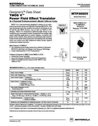
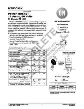
MOTOROLA Order this document SEMICONDUCTOR TECHNICAL DATA by MTP3055V/D Designer's Data Sheet MTP3055V TMOS V Motorola Preferred Device Power Field Effect Transistor N Channel Enhancement Mode Silicon Gate TMOS POWER FET TMOS V is a new technology designed to achieve an on resis- 12 AMPERES tance area product about one half that of standard MOSFETs. This 60 VOLTS... See More ⇒
MOTOROLA Order this document SEMICONDUCTOR TECHNICAL DATA by MTP3055V/D Designer's Data Sheet MTP3055V TMOS V Motorola Preferred Device Power Field Effect Transistor N Channel Enhancement Mode Silicon Gate TMOS POWER FET TMOS V is a new technology designed to achieve an on resis- 12 AMPERES tance area product about one half that of standard MOSFETs. This 60 VOLTS... See More ⇒
Detailed specifications: TP2907A, TP2907AR, TP2907R, TP2923, TP2924, TP2925, TP2926, TP3013, S8550, TP3053A, TP3250, TP3250A, TP3251, TP3251A, TP3390, TP3391, TP3391A
Keywords - TP3053 pdf specs
TP3053 cross reference
TP3053 equivalent finder
TP3053 pdf lookup
TP3053 substitution
TP3053 replacement
History: 2N218 | 2N2181 | TP2907AR | MPS4258A | 2SC5455 | KF508
🌐 : EN ES РУ
LIST
Last Update
BJT: GA1A4M | SBT42 | 2SA200-Y | 2SA200-O | 2SD882-Q | 2SD882-P
Popular searches
nce82h140 | 2n2369 equivalent | 2sd313 datasheet | k8a50d datasheet | 2sc381 | datasheet mosfet | 2sk2586 | 13005 transistor

