TR21 Datasheet. Specs and Replacement
Type Designator: TR21 📄📄
Material of Transistor: Si
Polarity: NPN
Absolute Maximum Ratings
Maximum Collector Power Dissipation (Pc): 0.36 W
Maximum Collector-Base Voltage |Vcb|: 40 V
Maximum Collector-Emitter Voltage |Vce|: 30 V
Maximum Emitter-Base Voltage |Veb|: 5 V
Maximum Collector Current |Ic max|: 0.5 A
Max. Operating Junction Temperature (Tj): 150 °C
Electrical Characteristics
Transition Frequency (ft): 250 MHz
Collector Capacitance (Cc): 8 pF
Forward Current Transfer Ratio (hFE), MIN: 60
Noise Figure, dB: -
📄📄 Copy
TR21 Substitution
- BJT ⓘ Cross-Reference Search
TR21 datasheet
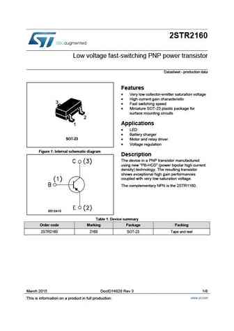
2STR2160 Low voltage fast-switching PNP power transistor Datasheet - production data Features Very low collector-emitter saturation voltage High current gain characteristic Fast switching speed Miniature SOT-23 plastic package for surface mounting circuits Applications LED Battery charger SOT-23 Motor and relay driver Voltage regulation... See More ⇒
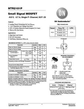
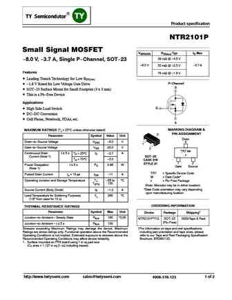
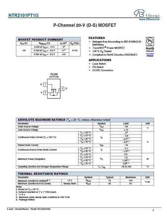
NTR2101P Small Signal MOSFET -8.0 V, -3.7 A, Single P-Channel, SOT-23 Features Leading Trench Technology for Low RDS(on) http //onsemi.com -1.8 V Rated for Low Voltage Gate Drive V(BR)DSS RDS(on) Typ ID Max SOT-23 Surface Mount for Small Footprint (3 x 3 mm) 39 mW @ -4.5 V This is a Pb-Free Device -8.0 V 52 mW @ -2.5 V -3.7 A Applications High Side Load Switch ... See More ⇒
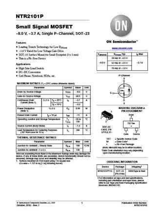
NTR2101P Small Signal MOSFET -8.0 V, -3.7 A, Single P-Channel, SOT-23 Features Leading Trench Technology for Low RDS(on) http //onsemi.com -1.8 V Rated for Low Voltage Gate Drive V(BR)DSS RDS(on) Typ ID Max SOT-23 Surface Mount for Small Footprint (3 x 3 mm) 39 mW @ -4.5 V This is a Pb-Free Device -8.0 V 52 mW @ -2.5 V -3.7 A Applications High Side Load Switch ... See More ⇒
Detailed specifications: TR07, TR08, TR09, TR1001A, TR1030A, TR1032A, TR-1033-1, TR1034A, BC548, TR-21C, TR24, TR310249, TR-3R38, TR-4R33, TR-5R38, TR-7R31, TR8004-4
Keywords - TR21 pdf specs
TR21 cross reference
TR21 equivalent finder
TR21 pdf lookup
TR21 substitution
TR21 replacement
BJT Parameters and How They Relate
History: KRC881T | KT683V | RN4985FS | RN2309 | MQ2369 | EN914 | RN2913FS
🌐 : EN ES РУ
LIST
Last Update
BJT: ZDT6705 | GA1L4Z | GA1A4M | SBT42 | 2SA200-Y | 2SA200-O
Popular searches
2sd388 | 2sc1400 | 2sd331 | 2sc1312 datasheet | 2sb647 | k3561 transistor | c3203 transistor | irfp450 equivalent
