2N5839 Datasheet. Specs and Replacement
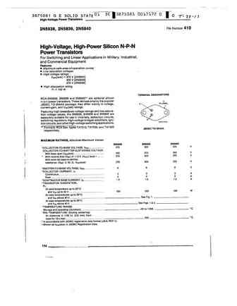
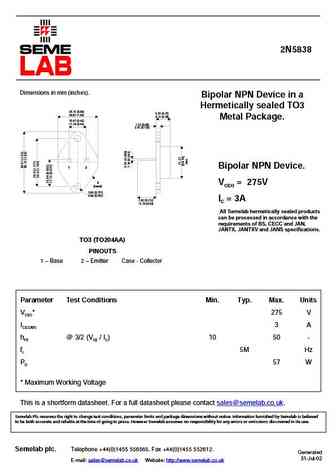
Type Designator: 2N5839 📄📄
Material of Transistor: Si
Polarity: NPN
Absolute Maximum Ratings
Maximum Collector Power Dissipation (Pc): 100 W
Maximum Collector-Base Voltage |Vcb|: 300 V
Maximum Collector-Emitter Voltage |Vce|: 275 V
Maximum Emitter-Base Voltage |Veb|: 6 V
Maximum Collector Current |Ic max|: 3 A
Max. Operating Junction Temperature (Tj): 200 °C
Electrical Characteristics
Transition Frequency (ft): 5 MHz
Forward Current Transfer Ratio (hFE), MIN: 10
Package: TO3
📄📄 Copy
2N5839 Substitution
- BJT ⓘ Cross-Reference Search
2N5839 datasheet
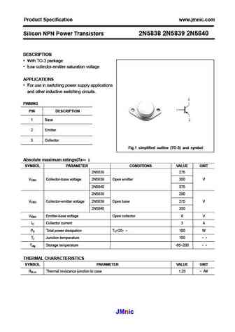
Product Specification www.jmnic.com Silicon NPN Power Transistors 2N5838 2N5839 2N5840 DESCRIPTION With TO-3 package Low collector-emitter saturation voltage APPLICATIONS For use in switching power supply applications and other inductive switching circuits. PINNING PIN DESCRIPTION 1 Base 2 Emitter 3 Collector Fig.1 simplified outline (TO-3) and symbol Absolute max... See More ⇒
Inchange Semiconductor Product Specification Silicon NPN Power Transistors 2N5838 2N5839 2N5840 DESCRIPTION With TO-3 package Low collector saturation voltage High breakdown voltage APPLICATIONS For use in switching power supply and other inductive switching circuits. PINNING PIN DESCRIPTION 1 Base 2 Emitter Fig.1 simplified outline (TO-3) and symbol 3 Collecto... See More ⇒
Detailed specifications: 2N5831, 2N5832, 2N5833, 2N5834, 2N5835, 2N5836, 2N5837, 2N5838, A1015, 2N583A, 2N584, 2N5840, 2N5841, 2N5842, 2N5843, 2N5844, 2N5845
Keywords - 2N5839 pdf specs
2N5839 cross reference
2N5839 equivalent finder
2N5839 pdf lookup
2N5839 substitution
2N5839 replacement
BJT Parameters and How They Relate
History: 2SA1576ART1 | KRC121M | 2N3923 | NB212HG | BD249C | RN2502 | 2N3815
🌐 : EN ES РУ
LIST
Last Update
BJT: ZDT6705 | GA1L4Z | GA1A4M | SBT42 | 2SA200-Y | 2SA200-O
Popular searches
2sc2078 transistor equivalent | 2sc2073 | a608 transistor | c536 transistor | 2n706 | 2n388 | 2n3645 | 2n1307
