TN5320A Specs and Replacement
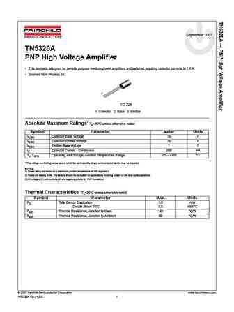
Type Designator: TN5320A
Material of Transistor: Si
Polarity: PNP
Absolute Maximum Ratings
Maximum Collector Power Dissipation (Pc): 1 W
Maximum Collector-Base Voltage |Vcb|: 75 V
Maximum Collector-Emitter Voltage |Vce|: 75 V
Maximum Emitter-Base Voltage |Veb|: 7 V
Maximum Collector Current |Ic max|: 0.5 A
Max. Operating Junction Temperature (Tj): 150 °C
Electrical Characteristics
Forward Current Transfer Ratio (hFE), MIN: 30
Package: TO-226
TN5320A Substitution
- BJT ⓘ Cross-Reference Search
TN5320A datasheet
September 2007 TN5320A PNP High Voltage Amplifier This device is designed for general purpose medium power amplifiers and switches requiring collector currents to 1.5 A. Sourced from Process 34. 1 TO-226 1. Collector 2. Base 3. Emitter Absolute Maximum Ratings* Ta=25 C unless otherwise noted Symbol Parameter Value Units VCBO Collector-Base Voltage 75 V VCEO Collector-Emitte... See More ⇒
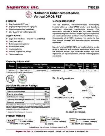
TN5325 N-Channel Enhancement-Mode Vertical DMOS FET Features General Description Low threshold (2.0V max.) This low threshold, enhancement-mode (normally-off) High input impedance and high gain transistor utilizes a vertical DMOS structure and Supertex s well-proven, silicon-gate manufacturing process. This Free from secondary breakdown combination produces a device ... See More ⇒
Detailed specifications: SD1398, SJ5436, SJ5437, SJ5439, STS8550, TN3019A, TN3440A, TN4033A, BC549, TN5415A, TN6705A, TN6707A, TN6716A, TN6718A, TN6719A, TN6725A, TN6727A
Keywords - TN5320A pdf specs
TN5320A cross reference
TN5320A equivalent finder
TN5320A pdf lookup
TN5320A substitution
TN5320A replacement


