STD1862L Datasheet. Specs and Replacement
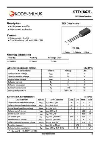
Type Designator: STD1862L 📄📄
SMD Transistor Code: STD1862
Material of Transistor: Si
Polarity: NPN
Absolute Maximum Ratings
Maximum Collector Power Dissipation (Pc): 1 W
Maximum Collector-Base Voltage |Vcb|: 30 V
Maximum Collector-Emitter Voltage |Vce|: 30 V
Maximum Emitter-Base Voltage |Veb|: 5 V
Maximum Collector Current |Ic max|: 2 A
Max. Operating Junction Temperature (Tj): 150 °C
Electrical Characteristics
Transition Frequency (ft): 170 MHz
Collector Capacitance (Cc): 48 pF
Forward Current Transfer Ratio (hFE), MIN: 100
Noise Figure, dB: -
Package: TO-92L
- BJT ⓘ Cross-Reference Search
STD1862L datasheet
..1. Size:193K auk
std1862l.pdf 

STD1862L NPN Silicon Transistor Descriptions PIN Connection Audio power amplifier High current application Features High current IC=2A Complementary pair with STB1277L TO -92L 1 Emitter 2 Collector 3 Base Ordering Information Type NO. Marking Package Code STD1862L STD1862 TO-92L Absolute maximum ratings (Ta=25 C) Characteristic Symbol Rati... See More ⇒
7.1. Size:224K auk
std1862.pdf 

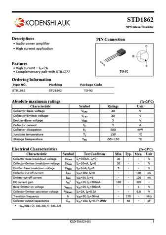
STD1862 NPN Silicon Transistor Descriptions PIN Connection Audio power amplifier C High current application B Features E High current IC=2A TO-92 Complementary pair with STB1277 Ordering Information Type NO. Marking Package Code STD1862 STD1862 TO-92 Absolute maximum ratings (Ta=25 C) Characteristic Symbol Ratings Unit Collector-Base voltag... See More ⇒
9.1. Size:630K 1
std180n4f6.pdf 

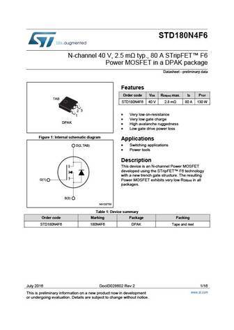
STD180N4F6 N-channel 40 V, 2.5 m typ., 80 A STripFET F6 Power MOSFET in a DPAK package Datasheet - preliminary data Features Order code V R max. I P DS DS(on) D TOT STD180N4F6 40 V 2.8 m 80 A 130 W Very low on-resistance Very low gate charge High avalanche ruggedness Low gate drive power loss Figure 1 Internal schematic diagram Applications ... See More ⇒
9.2. Size:1107K st
stb18nf25 std18nf25.pdf 

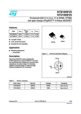
STB18NF25 STD18NF25 N-channel 250 V, 0.14 , 17 A DPAK, D2PAK low gate charge STripFET II Power MOSFET Features RDS(on) Type VDSS ID PTOT max STB18NF25 250 V ... See More ⇒
9.3. Size:752K st
std18n55m5 stp18n55m5.pdf 

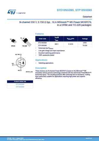
STD18N55M5, STP18N55M5 Datasheet N-channel 550 V, 0.150 typ., 16 A MDmesh M5 Power MOSFETs in a DPAK and TO-220 packages Features VDS @ TAB RDS(on)max. Order code Package TAB Tjmax. 3 2 STD18N55M5 DPAK 1 600 V 0.192 3 2 STP18N55M5 TO-220 DPAK TO-220 1 Extremely low RDS(on) Low gate charge and input capacitance Excellent switching performance D(2, TA... See More ⇒
9.4. Size:242K st
std1802.pdf 

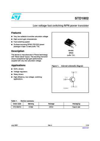
STD1802 Low voltage fast-switching NPN power transistor Features Very low collector to emitter saturation voltage High current gain characteristic Fast-switching speed Surface-mounting DPAK (TO-252) power 3 package in tape & reel (suffix T4) 1 TO-252 Description DPAK The device is manufactured in Planar technology (suffix T4 ) with Base Island l... See More ⇒
9.5. Size:1015K st
stb18n65m5 std18n65m5.pdf 

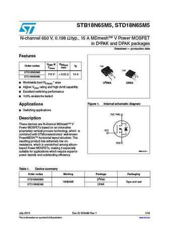
STB18N65M5, STD18N65M5 N-channel 650 V, 0.198 typ., 15 A MDmesh V Power MOSFET in D PAK and DPAK packages Datasheet production data Features VDSS @ RDS(on) Order codes ID TAB TJmax max TAB STB18N65M5 710 V ... See More ⇒
9.6. Size:304K st
std18nf03l.pdf 

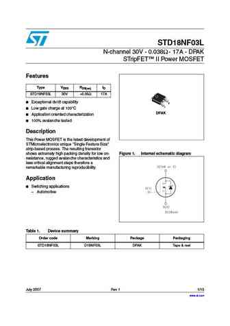
STD18NF03L N-channel 30V - 0.038 - 17A - DPAK STripFET II Power MOSFET Features Type VDSS RDS(on) ID STD18NF03L 30V ... See More ⇒
9.7. Size:237K st
std1805.pdf 

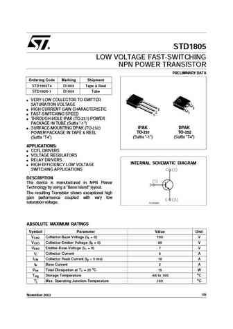
STD1805 LOW VOLTAGE FAST-SWITCHING NPN POWER TRANSISTOR PRELIMINARY DATA Ordering Code Marking Shipment STD1805T4 D1805 Tape & Reel STD1805-1 D1805 Tube VERY LOW COLLECTOR TO EMITTER SATURATION VOLTAGE 3 HIGH CURRENT GAIN CHARACTERISTIC 3 2 1 FAST-SWITCHING SPEED 1 THROUGH-HOLE IPAK (TO-251) POWER PACKAGE IN TUBE (Suffix "-1") IPAK DPAK SURFACE-MOUNTING DPAK (TO-252) ... See More ⇒
9.8. Size:247K st
std1802t4-a.pdf 

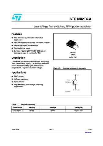
STD1802T4-A Low voltage fast-switching NPN power transistor Features This device is qualified for automotive application Very low collector to emitter saturation voltage High current gain characteristic 3 Fast-switching speed 1 Surface-mounting DPAK (TO-252) power TO-252 package in tape & reel (suffix T4) DPAK (suffix T4 ) Description The device ... See More ⇒
9.9. Size:1247K st
stb18n55m5 std18n55m5 stf18n55m5 stp18n55m5.pdf 

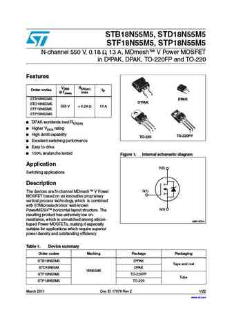
STB18N55M5, STD18N55M5 STF18N55M5, STP18N55M5 N-channel 550 V, 0.18 , 13 A, MDmesh V Power MOSFET in D PAK, DPAK, TO-220FP and TO-220 Features VDSS RDS(on) Order codes ID 3 @TJmax max 1 3 1 STB18N55M5 DPAK D PAK STD18N55M5 550 V ... See More ⇒
9.10. Size:106K samhop
stu1855pl std1855pl.pdf 

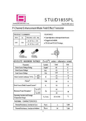
S TU/D1855P L S amHop Microelectronics C orp. Arp,20 2005 ver1.1 P-Channel E nhancement Mode Field E ffect Transistor PR ODUC T S UMMAR Y FEATUR ES R DS (ON) ( m ) Max VDS S ID S uper high dense cell design for low R DS (ON). R ugged and reliable. 68 @ VGS =-10V -55V -15A TO-252 and TO-251 Package. 85 @ VGS = -4.5V D D G G S STU SERIES STD SERIES TO-252AA(D-PAK) TO-251(l-PA... See More ⇒
9.11. Size:222K inchange semiconductor
std1802.pdf 
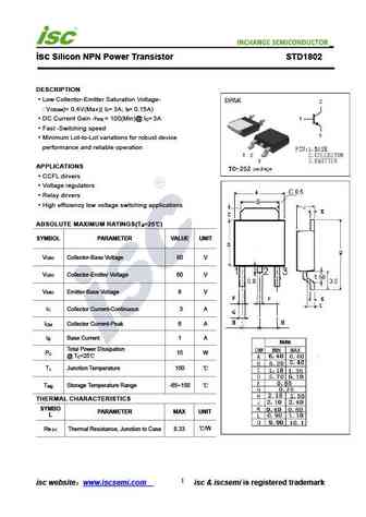
isc Silicon NPN Power Transistor STD1802 DESCRIPTION Low Collector-Emitter Saturation Voltage- V )= 0.4V(Max)( I = 3A; I = 0.15A) CE(sat C B DC Current Gain -h = 100(Min)@ I = 3A FE C Fast -Switching speed Minimum Lot-to-Lot variations for robust device performance and reliable operation APPLICATIONS CCFL dirvers Voltage regulators Relay dirvers High efficiency l... See More ⇒
9.12. Size:208K inchange semiconductor
std18n65m5.pdf 
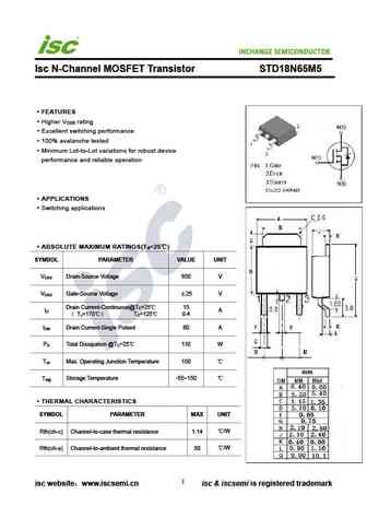
INCHANGE Semiconductor Isc N-Channel MOSFET Transistor STD18N65M5 FEATURES Higher V rating DSS Excellent switching performance 100% avalanche tested Minimum Lot-to-Lot variations for robust device performance and reliable operation APPLICATIONS Switching applications ABSOLUTE MAXIMUM RATINGS(T =25 ) a SYMBOL PARAMETER VALUE UNIT V Drain-Source Voltage 650 V DSS ... See More ⇒
9.13. Size:262K inchange semiconductor
std18n55m5.pdf 
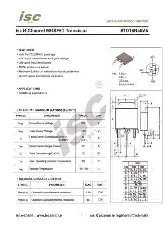
Isc N-Channel MOSFET Transistor STD18N55M5 FEATURES With To-252(DPAK) package Low input capacitance and gate charge Low gate input resistance 100% avalanche tested Minimum Lot-to-Lot variations for robust device performance and reliable operation APPLICATIONS Switching applications ABSOLUTE MAXIMUM RATINGS(T =25 ) a SYMBOL PARAMETER VALUE UNIT V Drain-Source Vol... See More ⇒
Detailed specifications: STD123ASF, STD123SF, STD123U, STD123UF, STD129, STD1664, STD1766, STD1862, BC549, STD361, STD6528EF, STD6528S, STN2222, STN2222A, STN2222AS, STN2222ASF, STN2222S
Keywords - STD1862L pdf specs
STD1862L cross reference
STD1862L equivalent finder
STD1862L pdf lookup
STD1862L substitution
STD1862L replacement
