4126 Specs and Replacement
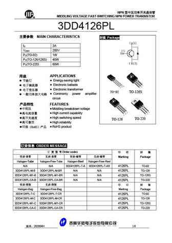
Type Designator: 4126
Material of Transistor: Si
Polarity: NPN
Absolute Maximum Ratings
Maximum Collector Power Dissipation (Pc): 40 W
Maximum Collector-Base Voltage |Vcb|: 400 V
Maximum Collector-Emitter Voltage |Vce|: 200 V
Maximum Emitter-Base Voltage |Veb|: 7 V
Maximum Collector Current |Ic max|: 3 A
Max. Operating Junction Temperature (Tj): 150 °C
Electrical Characteristics
Transition Frequency (ft): 4 MHz
Forward Current Transfer Ratio (hFE), MIN: 10
Noise Figure, dB: -
Package: TO-126
- BJT ⓘ Cross-Reference Search
4126 datasheet
..1. Size:106K utc
4126.pdf 

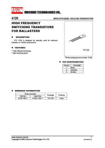
UNISONIC TECHNOLOGIES CO., 4126 NPN EPITAXIAL SILICON TRANSISTOR HIGH FREQUENCY SWITCHING TRANSISTORS FOR BALLASTERS . DESCRIPTION UTC 4126 is designed for specially used for electronic 1 ballasters in 110VAC environment. FEATURES TO-126 * Triple diffused technology. * High switching speed *Pb-free plating product number 4126L PIN CONFIGURATION PIN NO. PIN NA... See More ⇒
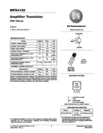
0.2. Size:58K motorola
mps4126rev0.pdf 

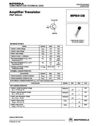
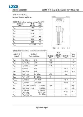
MOTOROLA Order this document SEMICONDUCTOR TECHNICAL DATA by MPS4126/D Amplifier Transistor PNP Silicon MPS4126 COLLECTOR 3 2 BASE 1 EMITTER 1 2 3 CASE 29 04, STYLE 1 TO 92 (TO 226AA) MAXIMUM RATINGS Rating Symbol Value Unit Collector Emitter Voltage VCE 25 Vdc Collector Base Voltage VCB 25 Vdc Emitter Base Voltage VEB 4.0 Vdc Collector Current Co... See More ⇒
0.3. Size:165K motorola
2n4125 2n4126.pdf 

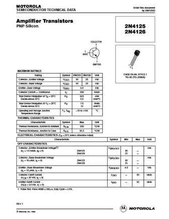
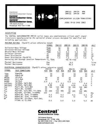
MOTOROLA Order this document SEMICONDUCTOR TECHNICAL DATA by 2N4125/D Amplifier Transistors PNP Silicon 2N4125 2N4126 COLLECTOR 3 2 BASE 1 EMITTER 1 2 3 MAXIMUM RATINGS CASE 29 04, STYLE 1 Rating Symbol 2N4125 2N4126 Unit TO 92 (TO 226AA) Collector Emitter Voltage VCEO 30 25 Vdc Collector Base Voltage VCBO 30 25 Vdc Emitter Base Voltage VEBO 4.0 Vdc Collector... See More ⇒
0.4. Size:48K philips
2n4126 cnv 2.pdf 

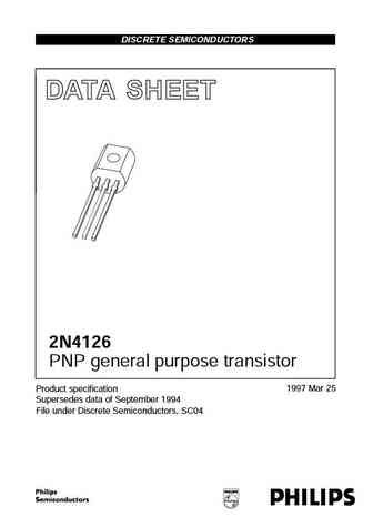
DISCRETE SEMICONDUCTORS DATA SHEET book, halfpage M3D186 2N4126 PNP general purpose transistor 1997 Mar 25 Product specification Supersedes data of September 1994 File under Discrete Semiconductors, SC04 Philips Semiconductors Product specification PNP general purpose transistor 2N4126 FEATURES PINNING Low current (max. 200 mA) PIN DESCRIPTION Low voltage (max. 25 V). 1... See More ⇒
0.5. Size:66K sanyo
2sk4126.pdf 

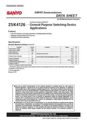
Ordering number ENA0748A 2SK4126 SANYO Semiconductors DATA SHEET N-Channel Silicon MOSFET General-Purpose Switching Device 2SK4126 Applications Features Low ON-resistance, low input capacitance, ultrahigh-speed switching. Adoption of high reliability HVP process. Avalanche resistance guarantee. Specifications Absolute Maximum Ratings at Ta=25 C Parameter Symbol Condi... See More ⇒
0.6. Size:81K fairchild semi
2n4126 mmbt4126.pdf 

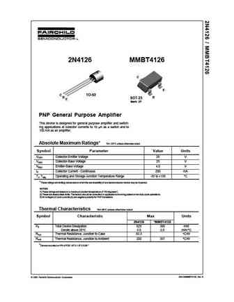
2N4126 MMBT4126 C E C TO-92 B B SOT-23 E Mark ZF PNP General Purpose Amplifier This device is designed for general purpose amplifier and switch- ing applications at collector currents to 10 A as a switch and to 100 mA as an amplifier. Absolute Maximum Ratings* TA = 25 C unless otherwise noted Symbol Parameter Value Units VCEO Collector-Emitter Voltage 25 V VCBO Collector-Base... See More ⇒
0.7. Size:44K fairchild semi
kst4126.pdf 

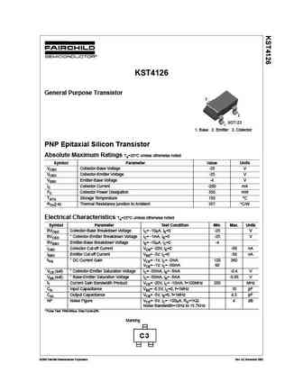
KST4126 General Purpose Transistor 3 2 SOT-23 1 1. Base 2. Emitter 3. Collector PNP Epitaxial Silicon Transistor Absolute Maximum Ratings Ta=25 C unless otherwise noted Symbol Parameter Value Units VCBO Collector-Base Voltage -25 V VCEO Collector-Emitter Voltage -25 V VEBO Emitter-Base Voltage -4 V IC Collector Current -200 mA PC Collector Power Dissipation 350 mW TSTG Storage ... See More ⇒
0.8. Size:96K siemens
smbt4126.pdf 

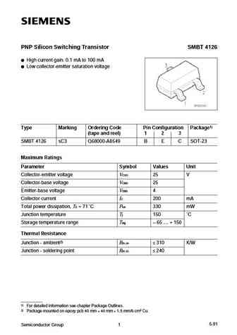
PNP Silicon Switching Transistor SMBT 4126 High current gain 0.1 mA to 100 mA Low collector-emitter saturation voltage Type Marking Ordering Code Pin Configuration Package1) (tape and reel) 1 2 3 SMBT 4126 sC3 Q68000-A8549 B E C SOT-23 Maximum Ratings Parameter Symbol Values Unit Collector-emitter voltage VCE0 25 V Collector-base voltage VCB0 25 Emitter-base voltage VEB0 4 Collect... See More ⇒
0.9. Size:268K vishay
si4126dy.pdf 

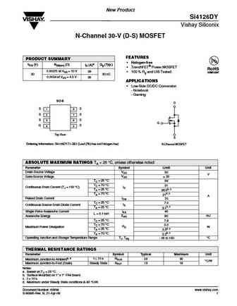
New Product Si4126DY Vishay Siliconix N-Channel 30-V (D-S) MOSFET FEATURES PRODUCT SUMMARY Halogen-free VDS (V) RDS(on) ( ) ID (A)a Qg (Typ.) TrenchFET Power MOSFET RoHS 0.00275 at VGS = 10 V 39 100 % Rg and UIS Tested COMPLIANT 30 30 nC 0.0034 at VGS = 4.5 V 35 APPLICATIONS Low-Side DC/DC Conversion - Notebook - Gaming SO-8 D SD 1 8 SD ... See More ⇒
0.11. Size:27K diodes
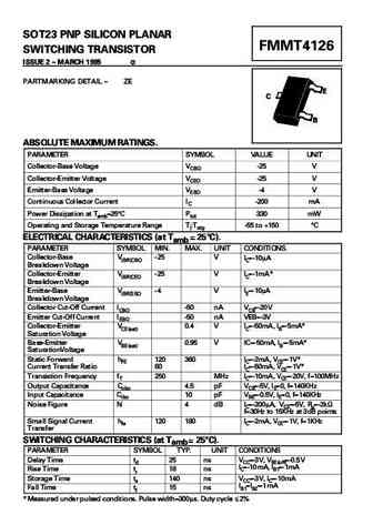
fmmt4126.pdf 

SOT SI I O A A T 6 S IT HI T A SISTO ISS A H T I D T I A SO T A I ATI S T V IT II V I V V II i V I V V i V I V V i II I Di i i T i T T T T I A HA A T ISTI S a Ta T I IT DITI II V V I V I II i V V I V I i V V I V I II I V V i I V V II i V V I I i V I i V V I I i V I i I V V T i I V V T i i T I V V i V V I ... See More ⇒
0.12. Size:118K diodes
mmst4126.pdf 

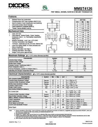
MMST4126 PNP SMALL SIGNAL SURFACE MOUNT TRANSISTOR Features Epitaxial Planar Die Construction A SOT-323 Complementary NPN Type Available (MMST4124) C Dim Min Max Ideal for Medium Power Amplification and Switching A 0.25 0.40 Ultra-Small Surface Mount Package B C B 1.15 1.35 Lead Free/RoHS Compliant (Note 2) "Green" Device (Notes 3 and 4) C 2.00 ... See More ⇒
0.13. Size:164K diodes
mmdt4126.pdf 

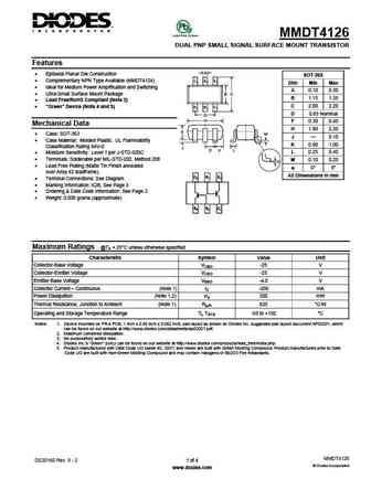
MMDT4126 DUAL PNP SMALL SIGNAL SURFACE MOUNT TRANSISTOR Features A Epitaxial Planar Die Construction SOT-363 Complementary NPN Type Available (MMDT4124) C2 B1 E1 Dim Min Max Ideal for Medium Power Amplification and Switching A 0.10 0.30 Ultra-Small Surface Mount Package B C B 1.15 1.35 Lead Free/RoHS Compliant (Note 3) C 2.00 2.20 "Green" Devic... See More ⇒
0.14. Size:339K diodes
mmbt4126.pdf 

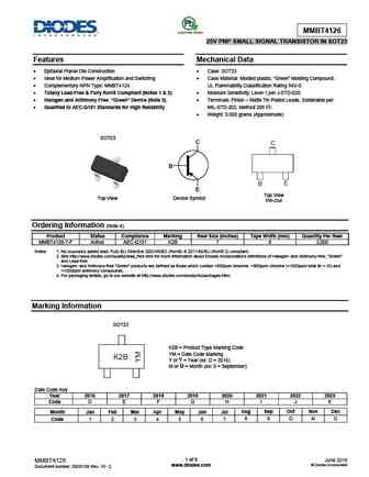
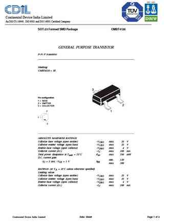
MMBT4126 25V PNP SMALL SIGNAL TRANSISTOR IN SOT23 Features Mechanical Data Epitaxial Planar Die Construction Case SOT23 Ideal for Medium Power Amplification and Switching Case Material Molded plastic, Green Molding Compound; Complementary NPN Type MMBT4124 UL Flammability Classification Rating 94V-0 Totally Lead-Free & Fully RoHS Compliant (Notes 1 &... See More ⇒
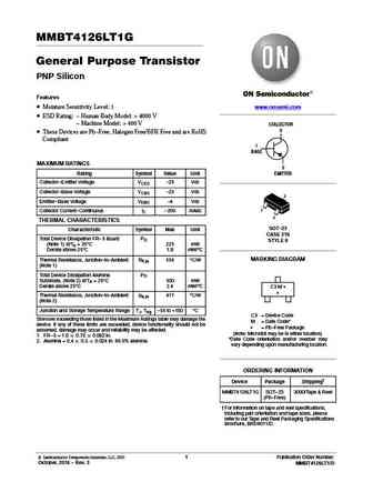
0.15. Size:154K onsemi
mmbt4126lt1.pdf 

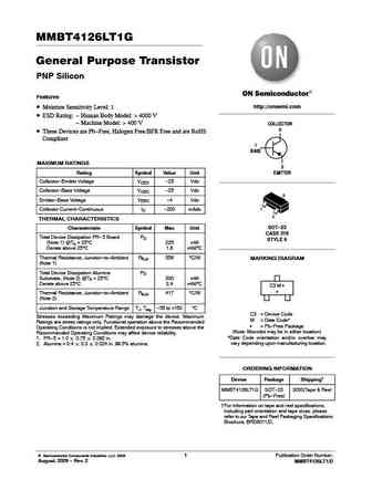
MMBT4126LT1G General Purpose Transistor PNP Silicon Features http //onsemi.com Moisture Sensitivity Level 1 ESD Rating - Human Body Model > 4000 V - Machine Model > 400 V COLLECTOR 3 These Devices are Pb-Free, Halogen Free/BFR Free and are RoHS Compliant 1 BASE MAXIMUM RATINGS 2 Rating Symbol Value Unit EMITTER Collector-Emitter Voltage VCEO -25 Vdc Collector-Ba... See More ⇒
0.16. Size:183K onsemi
mmbt4126lt1g.pdf 

MMBT4126LT1G General Purpose Transistor PNP Silicon Features Moisture Sensitivity Level 1 www.onsemi.com ESD Rating - Human Body Model > 4000 V - Machine Model > 400 V COLLECTOR 3 These Devices are Pb-Free, Halogen Free/BFR Free and are RoHS Compliant 1 BASE MAXIMUM RATINGS 2 Rating Symbol Value Unit EMITTER Collector-Emitter Voltage VCEO -25 Vdc Collector-Base ... See More ⇒
0.17. Size:48K onsemi
mps4126-d.pdf 

MPS4126 Amplifier Transistor PNP Silicon Features This is a Pb-Free Device* http //onsemi.com COLLECTOR 3 MAXIMUM RATINGS 2 Rating Symbol Value Unit BASE Collector-Emitter Voltage VCE -25 Vdc 1 Collector-Base Voltage VCB -25 Vdc EMITTER Emitter-Base Voltage VEB -4.0 Vdc Collector Current - Continuous IC -200 mAdc Total Device Dissipation @ TA = 25 C PD 625 W Derate above... See More ⇒
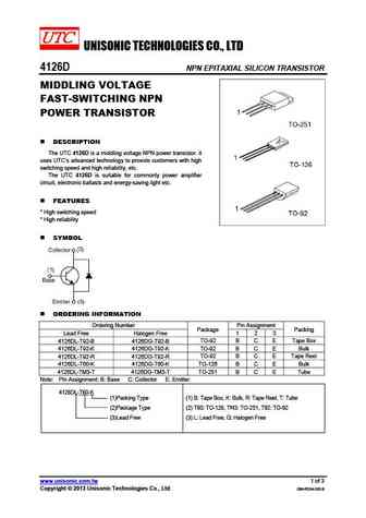
0.18. Size:147K utc
4126d.pdf 

UNISONIC TECHNOLOGIES CO., LTD 4126D NPN EPITAXIAL SILICON TRANSISTOR MIDDLING VOLTAGE FAST-SWITCHING NPN POWER TRANSISTOR DESCRIPTION The UTC 4126D is a middling voltage NPN power transistor. it uses UTC s advanced technology to provide customers with high switching speed and high reliability, etc. The UTC 4126D is suitable for commonly power amplifier circuit, electro... See More ⇒
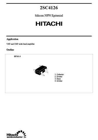
0.19. Size:47K hitachi
2sc4126.pdf 

2SC4126 Silicon NPN Epitaxial Application VHF and UHF wide band amplifier Outline MPAK-4 2 3 1 1. Collector 4 2. Emitter 3. Base 4. Emitter 2SC4126 Absolute Maximum Ratings (Ta = 25 C) Item Symbol Ratings Unit Collector to base voltage VCBO 15 V Collector to emitter voltage VCEO 11 V Emitter to base voltage VEBO 2V Collector current IC 50 mA Collector power dissipation PC... See More ⇒
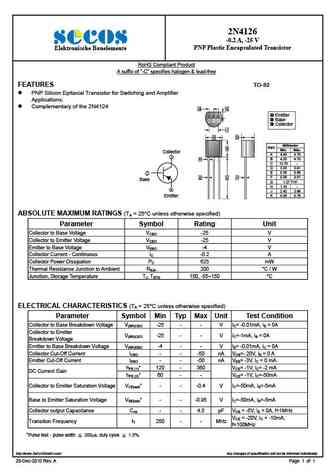
0.20. Size:109K secos
2n4126.pdf 

2N4126 -0.2 A, -25 V PNP Plastic Encapsulated Transistor Elektronische Bauelemente RoHS Compliant Product A suffix of -C specifies halogen & lead-free FEATURES TO-92 PNP Silicon Epitaxial Transistor for Switching and Amplifier Applications. Complementary of the 2N4124 G H Emitter Base Collector J A D Millimeter REF. B Min. Max. Collecto... See More ⇒
0.23. Size:457K aosemi
aod4126.pdf 

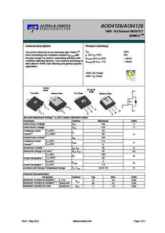
AOD4126/AOI4126 100V N-Channel MOSFET TM SDMOS General Description Product Summary 100V The AOD4126&AOI4126 are fabricated with SDMOSTM VDS ID (at VGS=10V) 43A trench technology that combines excellent RDS(ON) with low gate charge.The result is outstanding efficiency with RDS(ON) (at VGS=10V) ... See More ⇒
0.24. Size:457K aosemi
aoi4126.pdf 

AOD4126/AOI4126 100V N-Channel MOSFET TM SDMOS General Description Product Summary 100V The AOD4126&AOI4126 are fabricated with SDMOSTM VDS ID (at VGS=10V) 43A trench technology that combines excellent RDS(ON) with low gate charge.The result is outstanding efficiency with RDS(ON) (at VGS=10V) ... See More ⇒
0.25. Size:457K aosemi
aod4126 aoi4126.pdf 

AOD4126/AOI4126 100V N-Channel MOSFET TM SDMOS General Description Product Summary 100V The AOD4126&AOI4126 are fabricated with SDMOSTM VDS ID (at VGS=10V) 43A trench technology that combines excellent RDS(ON) with low gate charge.The result is outstanding efficiency with RDS(ON) (at VGS=10V) ... See More ⇒
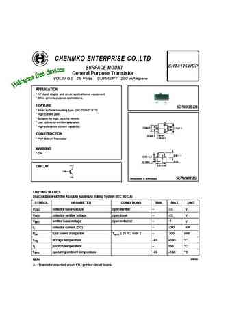
0.27. Size:157K chenmko
cht4126wgp.pdf 

CHENMKO ENTERPRISE CO.,LTD CHT4126WGP SURFACE MOUNT General Purpose Transistor VOLTAGE 25 Volts CURRENT 200 mAmpere APPLICATION * AF input stages and driver applicationon equipment. * Other general purpose applications. FEATURE SC-70/SOT-323 * Small surface mounting type. (SC-70/SOT-323) * High current gain. * Suitable for high packing density. * Low colloector-emitter saturation.... See More ⇒
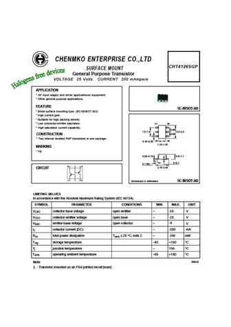
0.28. Size:149K chenmko
cht4126sgp.pdf 

CHENMKO ENTERPRISE CO.,LTD CHT4126SGP SURFACE MOUNT General Purpose Transistor VOLTAGE 25 Volts CURRENT 200 mAmpere APPLICATION * AF input stages and driver applicationon equipment. * Other general purpose applications. FEATURE SC-88/SOT-363 * Small surface mounting type. (SC-88/SOT-363) * High current gain. * Suitable for high packing density. * Low colloector-emitter saturation.... See More ⇒
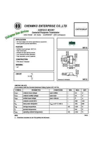
0.29. Size:186K chenmko
cht4126gp.pdf 

CHENMKO ENTERPRISE CO.,LTD CHT4126GP SURFACE MOUNT General Purpose Transistor VOLTAGE 25 Volts CURRENT 200 mAmpere APPLICATION * AF input stages and driver applicationon equipment. * Other general purpose applications. FEATURE SOT-23 * Surface mount package. (SOT-23) * High current gain. * Suitable for high packing density. * Low colloector-emitter saturation. (1) * High saturat... See More ⇒
0.33. Size:251K inchange semiconductor
aotf4126.pdf 
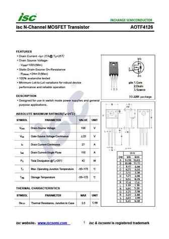
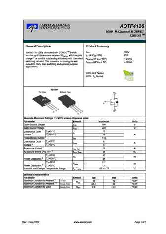
isc N-Channel MOSFET Transistor AOTF4126 FEATURES Drain Current I = 27A@ T =25 D C Drain Source Voltage- V =100V(Min) DSS Static Drain-Source On-Resistance R =24m (Max) DS(on) 100% avalanche tested Minimum Lot-to-Lot variations for robust device performance and reliable operation DESCRIPTION Designed for use in switch mode power supplies and general purpose... See More ⇒
0.34. Size:273K inchange semiconductor
2sk4126.pdf 
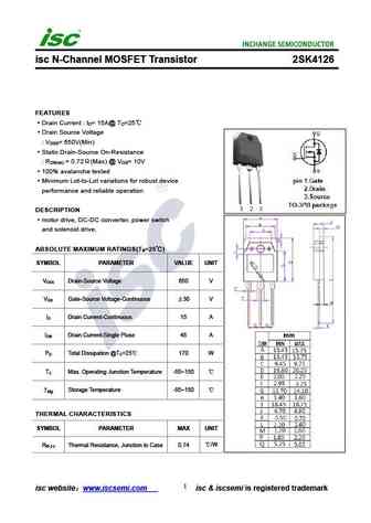
isc N-Channel MOSFET Transistor 2SK4126 FEATURES Drain Current I = 15A@ T =25 D C Drain Source Voltage V = 650V(Min) DSS Static Drain-Source On-Resistance R = 0.72 (Max) @ V = 10V DS(on) GS 100% avalanche tested Minimum Lot-to-Lot variations for robust device performance and reliable operation DESCRIPTION motor drive, DC-DC converter, power switch and soleno... See More ⇒
0.35. Size:265K inchange semiconductor
aod4126.pdf 
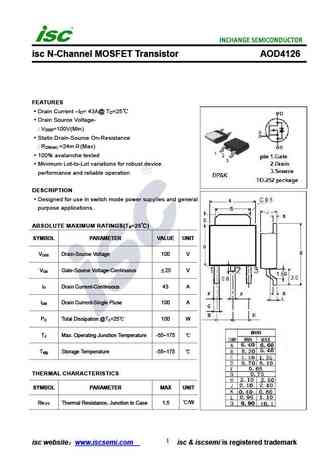
isc N-Channel MOSFET Transistor AOD4126 FEATURES Drain Current I = 43A@ T =25 D C Drain Source Voltage- V =100V(Min) DSS Static Drain-Source On-Resistance R =24m (Max) DS(on) 100% avalanche tested Minimum Lot-to-Lot variations for robust device performance and reliable operation DESCRIPTION Designed for use in switch mode power supplies and general purpose ... See More ⇒
0.36. Size:273K inchange semiconductor
aoi4126.pdf 
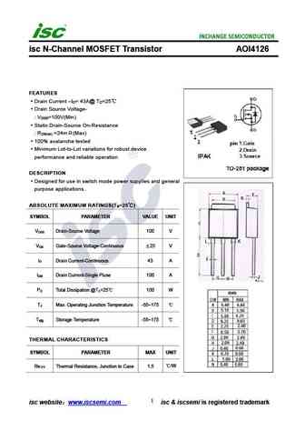
isc N-Channel MOSFET Transistor AOI4126 FEATURES Drain Current I = 43A@ T =25 D C Drain Source Voltage- V =100V(Min) DSS Static Drain-Source On-Resistance R =24m (Max) DS(on) 100% avalanche tested Minimum Lot-to-Lot variations for robust device performance and reliable operation DESCRIPTION Designed for use in switch mode power supplies and general purpose ... See More ⇒
Detailed specifications: SUT495J
, SUT497H
, SUT507EF
, SUT509EF
, SUT510EF
, SUT562EF
, SUT575EF
, 4124
, A733
, 4128
, 5302
, 13002AH
, 13003ADA
, 13003BS
, 13003DE
, 13003DF
, 13003DH
.
History: 2SB77A
| TSC966CW
Keywords - 4126 pdf specs
4126 cross reference
4126 equivalent finder
4126 pdf lookup
4126 substitution
4126 replacement
![]()


