STF22907GW Datasheet. Specs and Replacement
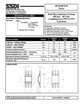
Type Designator: STF22907GW 📄📄
Material of Transistor: Si
Polarity: NPN*PNP
Absolute Maximum Ratings
Maximum Collector Power Dissipation (Pc): 0.5 W
Maximum Collector-Base Voltage |Vcb|: 60 V
Maximum Collector-Emitter Voltage |Vce|: 50 V
Maximum Emitter-Base Voltage |Veb|: 6 V
Maximum Collector Current |Ic max|: 0.6 A
Max. Operating Junction Temperature (Tj): 200 °C
Electrical Characteristics
Transition Frequency (ft): 200 MHz
Collector Capacitance (Cc): 8 pF
Forward Current Transfer Ratio (hFE), MIN: 50
Package: GW
📄📄 Copy
STF22907GW Substitution
- BJT ⓘ Cross-Reference Search
STF22907GW datasheet
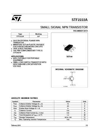
STF2222A SMALL SIGNAL NPN TRANSISTOR PRELIMINARY DATA Type Marking STF2222A 20F SILICON EPITAXIAL PLANAR NPN TRANSISTOR MINIATURE SOT-89 PLASTIC PACKAGE FOR SURFACE MOUNTING CIRCUITS TAPE & REEL PACKING THE PNP COMPLEMENTARY TYPE IS STF2907A APPLICATIONS SOT-89 WELL SUITABLE FOR PORTABLE EQUIPMENT SMALL LOAD SWITCH TRANSISTOR WITH HIGH GAIN AND LOW SATURATION VOLTAG... See More ⇒
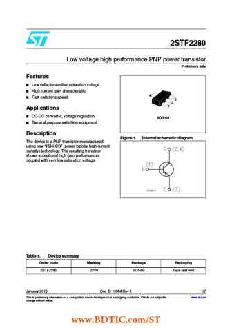
2STF2280 Low voltage high performance PNP power transistor Preliminary data Features Low collector-emitter saturation voltage High current gain characteristic 4 Fast switching speed 3 2 1 Applications DC-DC converter, voltage regulation SOT-89 General purpose switching equipment Description Figure 1. Internal schematic diagram The device is a PNP transistor ... See More ⇒
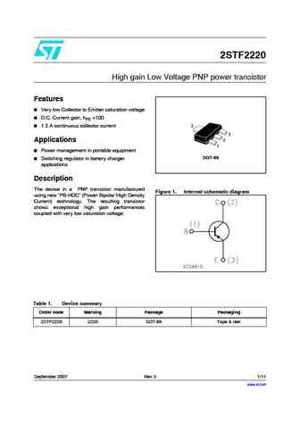
2STF2220 High gain Low Voltage PNP power transistor Features Very low Collector to Emitter saturation voltage D.C. Current gain, hFE >100 1.5 A continuous collector current Applications Power management in portable equipment SOT-89 Switching regulator in battery charger applications Description The device in a PNP transistor manufactured Figure 1. Internal sche... See More ⇒
Detailed specifications: STBV42D, STBV45D, STC03DE170HP, STC03DE170HV, STC03DE220HP, STC03DE220HV, STC04IE170HP, STC04IE170HV, A940, STI13005-1, STI13005H, STL128DFP, STL128DNFP, STLD128DNT4, STD01N, STD01P, STD127DT4
Keywords - STF22907GW pdf specs
STF22907GW cross reference
STF22907GW equivalent finder
STF22907GW pdf lookup
STF22907GW substitution
STF22907GW replacement
BJT Parameters and How They Relate
History: BFX93A | 2N358A | STBV42D | 2N3742 | BFX59 | ST2N2907A | 2N3586
🌐 : EN ES РУ
LIST
Last Update
BJT: ZDT6705 | GA1L4Z | GA1A4M | SBT42 | 2SA200-Y | 2SA200-O
Popular searches
2sa1015 | ksc3503 | c945 transistor datasheet | bt137 datasheet | 2n2907a datasheet | irfz24n | bd135 | d880
