NUS5530MN Datasheet. Specs and Replacement
Type Designator: NUS5530MN 📄📄
SMD Transistor Code: 5530
Material of Transistor: Si
Polarity: PNP
Absolute Maximum Ratings
Maximum Collector Power Dissipation (Pc): 2.75 W
Maximum Collector-Base Voltage |Vcb|: 55 V
Maximum Collector-Emitter Voltage |Vce|: 35 V
Maximum Emitter-Base Voltage |Veb|: 5 V
Maximum Collector Current |Ic max|: 2 A
Max. Operating Junction Temperature (Tj): 150 °C
Electrical Characteristics
Transition Frequency (ft): 100 MHz
Collector Capacitance (Cc): 85 pF
Forward Current Transfer Ratio (hFE), MIN: 100
Package: DFN8
NUS5530MN Substitution
- BJT ⓘ Cross-Reference Search
NUS5530MN datasheet
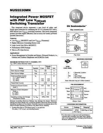
NUS5530MN Integrated Power MOSFET with PNP Low VCE(sat) Switching Transistor This integrated device represents a new level of safety and board-space reduction by combining the 20 V P-Channel FET with a http //onsemi.com PNP Silicon Low VCE(sat) switching transistor. This newly integrated product provides higher efficiency and accuracy for battery powered portable electronics. 1 8 Feat... See More ⇒
NUS5530MN Integrated Power MOSFET with PNP Low VCE(sat) Switching Transistor This integrated device represents a new level of safety and board-space reduction by combining the 20 V P-Channel FET with a http //onsemi.com PNP Silicon Low VCE(sat) switching transistor. This newly integrated product provides higher efficiency and accuracy for battery powered portable electronics. 1 8 Feat... See More ⇒
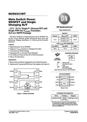
NUS5531MT Main Switch Power MOSFET and Single Charging BJT -12 V, -6.2 A, Single P-Channel FET with http //onsemi.com Single PNP low Vce(sat) Transistor, 3x3 mm WDFN Package MOSFET V(BR)DSS RDS(on) TYP ID MAX This device integrates one high performance power MOSFET and one low Vce(sat) transistor, greatly reducing the layout space and 32 mW @ -4.5 V -12 V -6.2 A optimizing charging... See More ⇒
Detailed specifications: NE02103, NE02107, NE02112, NE02132, NE02133, NE02135, NE73430, NE73435, 2SC1815, NXP3875G, NXP3875Y, NZT44H8, NZT45H8, N0501S, NJD1718T4G, NJD2873T4G, NJD35N04G
Keywords - NUS5530MN pdf specs
NUS5530MN cross reference
NUS5530MN equivalent finder
NUS5530MN pdf lookup
NUS5530MN substitution
NUS5530MN replacement


