NSVDTA123EM3T5G Specs and Replacement
Type Designator: NSVDTA123EM3T5G
SMD Transistor Code: 6H
Material of Transistor: Si
Polarity: Pre-Biased-PNP
Built in Bias Resistor R1 = 2.2 kOhm
Built in Bias Resistor R2 = 2.2 kOhm
Typical Resistor Ratio R1/R2 = 1
Absolute Maximum Ratings
Maximum Collector Power Dissipation (Pc): 0.26 W
Maximum Collector-Base Voltage |Vcb|: 50 V
Maximum Collector-Emitter Voltage |Vce|: 50 V
Maximum Collector Current |Ic max|: 0.1 A
Max. Operating Junction Temperature (Tj): 150 °C
Electrical Characteristics
Forward Current Transfer Ratio (hFE), MIN: 8
Package: SOT723
NSVDTA123EM3T5G Substitution
- BJT ⓘ Cross-Reference Search
NSVDTA123EM3T5G datasheet
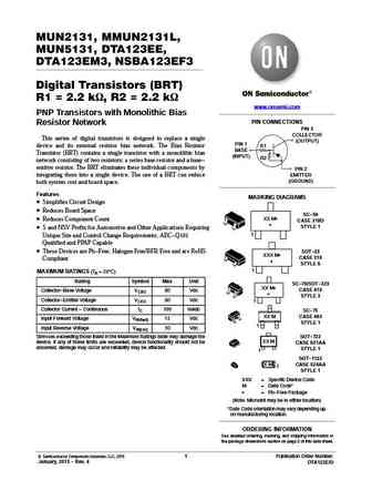
MUN2131, MMUN2131L, MUN5131, DTA123EE, DTA123EM3, NSBA123EF3 Digital Transistors (BRT) R1 = 2.2 kW, R2 = 2.2 kW www.onsemi.com PNP Transistors with Monolithic Bias PIN CONNECTIONS Resistor Network PIN 3 COLLECTOR This series of digital transistors is designed to replace a single (OUTPUT) PIN 1 device and its external resistor bias network. The Bias Resistor R1 BASE Transistor (B... See More ⇒

MUN2130, MMUN2130L, MUN5130, DTA113EE, DTA113EM3, NSBA113EF3 Digital Transistors (BRT) R1 = 1 kW, R2 = 1 kW www.onsemi.com PNP Transistors with Monolithic Bias PIN CONNECTIONS Resistor Network PIN 3 COLLECTOR This series of digital transistors is designed to replace a single (OUTPUT) PIN 1 device and its external resistor bias network. The Bias Resistor R1 BASE Transistor (BRT) ... See More ⇒

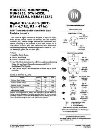
MUN2113, MMUN2113L, MUN5113, DTA144EE, DTA144EM3, NSBA144EF3 Digital Transistors (BRT) R1 = 47 kW, R2 = 47 kW www.onsemi.com PNP Transistors with Monolithic Bias PIN CONNECTIONS Resistor Network PIN 3 COLLECTOR This series of digital transistors is designed to replace a single (OUTPUT) PIN 1 device and its external resistor bias network. The Bias Resistor R1 BASE Transistor (BRT... See More ⇒

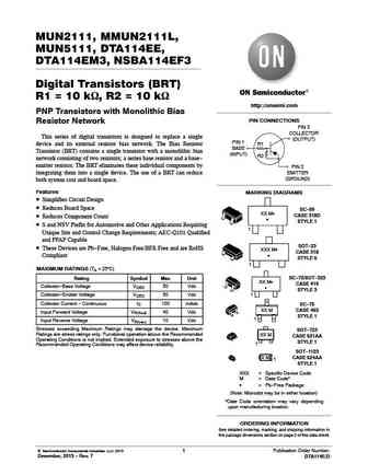
MUN2111, MMUN2111L, MUN5111, DTA114EE, DTA114EM3, NSBA114EF3 Digital Transistors (BRT) R1 = 10 kW, R2 = 10 kW http //onsemi.com PNP Transistors with Monolithic Bias PIN CONNECTIONS Resistor Network PIN 3 COLLECTOR This series of digital transistors is designed to replace a single (OUTPUT) PIN 1 device and its external resistor bias network. The Bias Resistor R1 BASE Transistor (... See More ⇒

Detailed specifications: NSVMMBT6517LT1G, NSVMMBT6520LT1G, NSVMMBTA05LT1G, NSVMMBTH10LT1G, NSVDTA113EM3T5G, NSVDTA114EET1G, NSVDTA114EM3T5G, NSVDTA115EET1G, BD222, NSVDTA143ZET1G, NSVDTA144EET1G, NSVDTA144WET1G, NSVDTC113EM3T5G, NSVDTC114YM3T5G, NSVDTC123EM3T5G, NSVDTC143ZET1G, NSVDTC143ZM3T5G
Keywords - NSVDTA123EM3T5G pdf specs
NSVDTA123EM3T5G cross reference
NSVDTA123EM3T5G equivalent finder
NSVDTA123EM3T5G pdf lookup
NSVDTA123EM3T5G substitution
NSVDTA123EM3T5G replacement
History: 2SC768 | NSVDTA114EM3T5G | 2SC366GR | NSVDTC113EM3T5G | 2SC751 | 2SC748
🌐 : EN ES РУ

LIST
Last Update
BJT: GA1A4M | SBT42 | 2SA200-Y | 2SA200-O | 2SD882-Q | 2SD882-P
Popular searches
a1693 datasheet | bdw94c equivalent | c2389 | c495 transistor | c5242 reemplazo | d667 transistor datasheet | hy1d datasheet | mp20a transistor