2N4899X Datasheet. Specs and Replacement
Type Designator: 2N4899X 📄📄
Material of Transistor: Si
Polarity: PNP
Absolute Maximum Ratings
Maximum Collector Power Dissipation (Pc): 25 W
Maximum Collector-Base Voltage |Vcb|: 60 V
Maximum Collector-Emitter Voltage |Vce|: 60 V
Maximum Emitter-Base Voltage |Veb|: 5 V
Maximum Collector Current |Ic max|: 4 A
Max. Operating Junction Temperature (Tj): 200 °C
Electrical Characteristics
Transition Frequency (ft): 3 MHz
Forward Current Transfer Ratio (hFE), MIN: 20
Package: TO-66
📄📄 Copy
2N4899X Substitution
- BJT ⓘ Cross-Reference Search
2N4899X datasheet
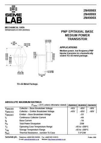
2N4898X 2N4899X 2N4900X MECHANICAL DATA Dimensions in mm (inches) PNP EPITAXIAL BASE MEDIUM POWER TRANSISTOR 6.35 (0.250) 8.64 (0.340) 3.68 (0.145) rad. 3.61 (0.142) max. 3.86 (0.145) rad. APPLICATIONS Medium power, low frequency PNP bipolar transistor in a hermetically sealed TO 66 metal package. 1.27 (0.050) 1.91 (0.750) 4.83 (0.190) 5.33 (0.210) 9.14 (0.360) min. ... See More ⇒
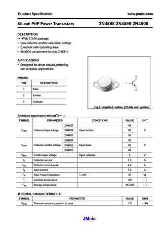
Product Specification www.jmnic.com Silicon PNP Power Transistors 2N4898 2N4899 2N4900 DESCRIPTION With TO-66 package Low collector-emitter saturation voltage Excellent safe operating area 2N4900 complement to type 2N4912 APPLICATIONS Designed for driver circuits,switching and amplifier applications PINNING PIN DESCRIPTION 1 Base 2 Emitter 3 Collector Fi... See More ⇒
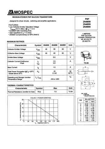
Inchange Semiconductor Product Specification Silicon PNP Power Transistors 2N4898 2N4899 2N4900 DESCRIPTION With TO-66 package Low collector saturation voltage Excellent safe operating area 2N4900 complement to type 2N4912 APPLICATIONS Designed for driver circuits,switching and amplifier applications PINNING PIN DESCRIPTION 1 Base 2 Emitter Fig.1 simplifi... See More ⇒
Detailed specifications: 2N4401L, 2N4401SC, 2N4403G, 2N4403SC, 2N4449UB, 2N4854U, 2N4897X, 2N4898X, BD336, 2N4900X, 2N4901SMD, 2N4910XSMD, 2N4910XSMD05, 2N4911XSMD, 2N4911XSMD05, 2N4918G, 2N4919G
Keywords - 2N4899X pdf specs
2N4899X cross reference
2N4899X equivalent finder
2N4899X pdf lookup
2N4899X substitution
2N4899X replacement
BJT Parameters and How They Relate
History: 2SC1116A | 2N3942 | 2N284
🌐 : EN ES РУ
LIST
Last Update
BJT: ZDT6705 | GA1L4Z | GA1A4M | SBT42 | 2SA200-Y | 2SA200-O
Popular searches
2n5457 equivalent | 2sc945 replacement | 9014 transistor | irfp260n datasheet | irfp250m | 2sk1058 | ss8550 | mje15033

