2SA1815 Datasheet. Specs and Replacement
Type Designator: 2SA1815 📄📄
SMD Transistor Code: JS3_JS4_JS5
Material of Transistor: Si
Polarity: PNP
Absolute Maximum Ratings
Maximum Collector Power Dissipation (Pc): 0.25 W
Maximum Collector-Base Voltage |Vcb|: 15 V
Maximum Collector-Emitter Voltage |Vce|: 12 V
Maximum Emitter-Base Voltage |Veb|: 3 V
Maximum Collector Current |Ic max|: 0.05 A
Max. Operating Junction Temperature (Tj): 150 °C
Electrical Characteristics
Transition Frequency (ft): 700 MHz
Collector Capacitance (Cc): 1.6 pF
Forward Current Transfer Ratio (hFE), MIN: 60
Noise Figure, dB: -
Package: SOT323
📄📄 Copy
- BJT ⓘ Cross-Reference Search
2SA1815 datasheet
..1. Size:70K sanyo
2sa1815.pdf 

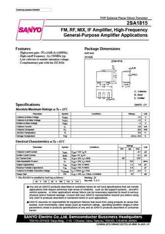
Ordering number EN4625 PNP Epitaxial Planar Silicon Transistor 2SA1815 FM, RF, MIX, IF Amplifier, High-Frequency General-Purpose Amplifier Applications Features Package Dimensions High power gain PG=25dB (f=100MHz). unit mm High cutoff frequency ; fT=750MHz typ. 2018A Low collector-to-emitter saturation voltage. [2SA1815] Complementary pair with the 2SC4432. C C... See More ⇒
..2. Size:903K kexin
2sa1815.pdf 

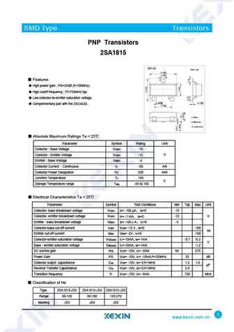
SMD Type Transistors PNP Transistors 2SA1815 SOT-23 Unit mm 2.9+0.1 -0.1 +0.1 0.4 -0.1 Features 3 High power gain PG=25dB (f=100MHz). High cutoff frequency ; fT=750MHz typ. Low collector-to-emitter saturation voltage. 1 2 +0.1 +0.05 0.95 -0.1 0.1 -0.01 Complementary pair with the 2SC4432. 1.9+0.1 -0.1 1.Base 2.Emitter 3.collector Absolute Max... See More ⇒
8.2. Size:84K sanyo
2sa1814.pdf 

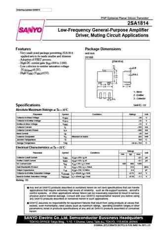
Ordering number EN3973 PNP Epitaxial Planar Silicon Transistor 2SA1814 Low-Frequency General-Purpose Amplifier Driver, Muting Circuit Applications Features Package Dimensions Very small-sized package permitting 2SA1814- unit mm applied sets to be made smaller and slimmer. 2018B Adoption of FBET process. [2SA1814] High DC current gain (hFE=500 to 1200). Low collector... See More ⇒
8.3. Size:83K sanyo
2sa1813.pdf 

Ordering number EN3972 PNP Epitaxial Planar Silicon Transistor 2SA1813 Low-Frequency General-Purpose Amplifier Driver, Muting Circuit Applications Features Package Dimensions Very small-sized package permitting 2SA1813- unit mm applied sets to be made smaller and slimmer. 2059A Adoption of FBET process. [2SA1813] High DC current gain (hFE=500 to 1200). Low collector... See More ⇒
8.4. Size:250K rohm
2sa1812 2sa1727 2sa1776.pdf 

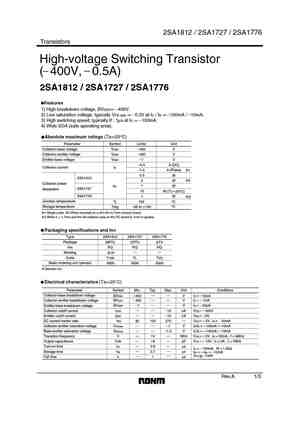
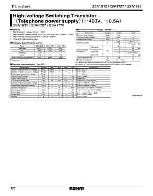
2SA1812 / 2SA1727 / 2SA1776 Transistors High-voltage Switching Transistor ( 400V, 0.5A) 2SA1812 / 2SA1727 / 2SA1776 Features 1) High breakdown voltage, BVCEO= 400V. 2) Low saturation voltage, typically VCE (sat) = 0.3V at IC / IB = 100mA / 10mA. 3) High switching speed, typically tf 1 s at IC = 100mA. 4) Wide SOA (safe operating area). Absolute maximum ratings (Ta=25 C) Paramete... See More ⇒
8.6. Size:25K panasonic
2sa1816 e.pdf 

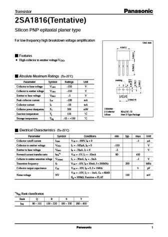
Transistor 2SA1816(Tentative) Silicon PNP epitaxial planer type For low-frequency high breakdown voltage amplification Unit mm 4.0 0.2 Features High collector to emitter voltage VCEO. Absolute Maximum Ratings (Ta=25 C) marking Parameter Symbol Ratings Unit 1 2 3 Collector to base voltage VCBO 150 V Collector to emitter voltage VCEO 150 V Emitter to base voltage VEBO 5... See More ⇒
8.7. Size:21K panasonic
2sa1816.pdf 

Transistor 2SA1816(Tentative) Silicon PNP epitaxial planer type For low-frequency high breakdown voltage amplification Unit mm 4.0 0.2 Features High collector to emitter voltage VCEO. Absolute Maximum Ratings (Ta=25 C) marking Parameter Symbol Ratings Unit 1 2 3 Collector to base voltage VCBO 150 V Collector to emitter voltage VCEO 150 V Emitter to base voltage VEBO 5... See More ⇒
8.8. Size:32K hitachi
2sa1810.pdf 

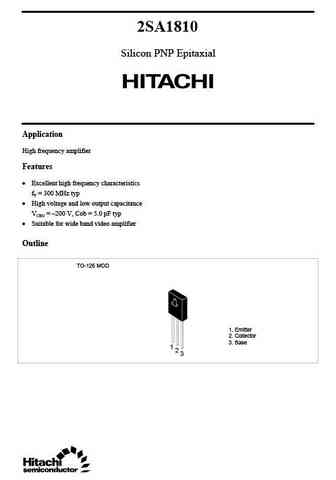
2SA1810 Silicon PNP Epitaxial Application High frequency amplifier Features Excellent high frequency characteristics fT = 300 MHz typ High voltage and low output capacitance VCEO = 200 V, Cob = 5.0 pF typ Suitable for wide band video amplifier Outline TO-126 MOD 1. Emitter 2. Collector 3. Base 1 2 3 2SA1810 Absolute Maximum Ratings (Ta = 25 C) Item Symbol Ra... See More ⇒
8.9. Size:1133K kexin
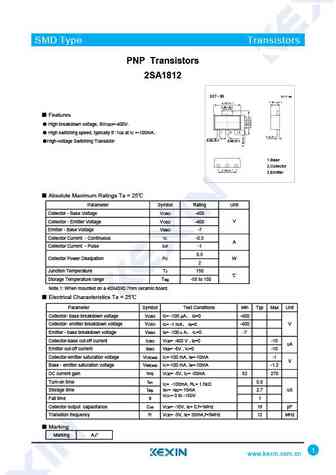
2sa1812.pdf 

SMD Type Transistors PNP Transistors 2SA1812 1.70 0.1 Features High breakdown voltage, BVCEO=-400V. High switching speed, typically tf 1us at IC =-100mA. 0.42 0.1 0.46 0.1 High-voltage Switching Transistor 1.Base 2.Collector 3.Emitter Absolute Maximum Ratings Ta = 25 Parameter Symbol Rating Unit Collector - Base Voltage VCBO -400 Collector - Emitter V... See More ⇒
8.10. Size:1036K kexin
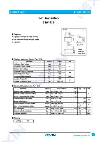
2sa1813.pdf 

SMD Type Transistors PNP Transistors 2SA1813 Features High DC current gain (hFE=500 to 1200). Low collector-to-emitter saturation voltage High VEBO 1 Base 2 Emitter 3 Colletor Absolute Maximum Ratings Ta = 25 Parameter Symbol Rating Unit Collector - Base Voltage VCBO -30 Collector - Emitter Voltage VCEO -25 V Emitter - Base Voltage VEBO -15 Collector... See More ⇒
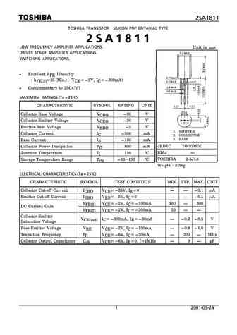
Detailed specifications: 2SA1805O, 2SA1805R, 2SA1806, 2SA181, 2SA1810, 2SA1810B, 2SA1810C, 2SA1811, 2SD313, 2SA1815-3, 2SA1815-4, 2SA1815-5, 2SA182, 2SA1822, 2SA183, 2SA1832, 2SA1837
Keywords - 2SA1815 pdf specs
2SA1815 cross reference
2SA1815 equivalent finder
2SA1815 pdf lookup
2SA1815 substitution
2SA1815 replacement
