TK10A50D Datasheet. Specs and Replacement
Type Designator: TK10A50D 📄📄
Type of Transistor: MOSFET
Type of Control Channel: N-Channel
Absolute Maximum Ratings
Pd ⓘ - Maximum Power Dissipation: 45 W
|Vds|ⓘ - Maximum Drain-Source Voltage: 500 V
|Vgs|ⓘ - Maximum Gate-Source Voltage: 30 V
|Id| ⓘ - Maximum Drain Current: 10 A
Tj ⓘ - Maximum Junction Temperature: 150 °C
Electrical Characteristics
tr ⓘ - Rise Time: 25 nS
Cossⓘ - Output Capacitance: 100 pF
RDSonⓘ - Maximum Drain-Source On-State Resistance: 0.72 Ohm
Package: TO220SIS
📄📄 Copy
TK10A50D substitution
- MOSFET ⓘ Cross-Reference Search
TK10A50D datasheet
tk10a50d.pdf
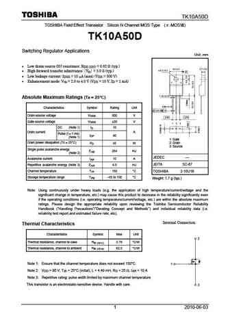
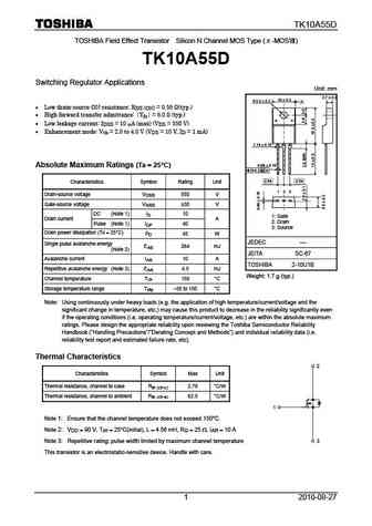
TK10A50D TOSHIBA Field Effect Transistor Silicon N Channel MOS Type ( -MOS ) TK10A50D Switching Regulator Applications Unit mm Low drain-source ON-resistance RDS (ON) = 0.62 (typ.) High forward transfer admittance Yfs = 5.0 S (typ.) Low leakage current IDSS = 10 A (max) (VDS = 500 V) Enhancement mode Vth = 2.0 to 4.0 V (VDS = 10 V, ID = 1 mA) ... See More ⇒
tk10a50d.pdf
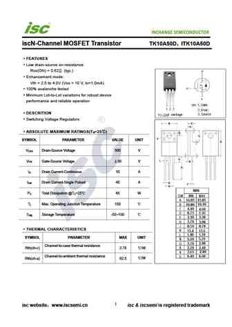
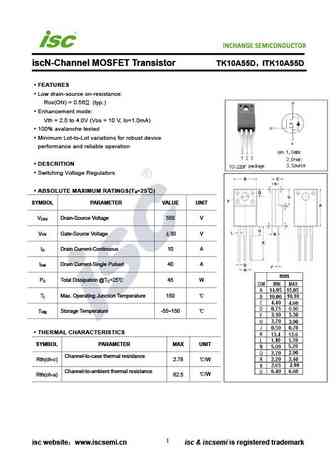
INCHANGE Semiconductor iscN-Channel MOSFET Transistor TK10A50D ITK10A50D FEATURES Low drain-source on-resistance RDS(ON) = 0.62 (typ.) Enhancement mode Vth = 2.0 to 4.0V (VDS = 10 V, ID=1.0mA) 100% avalanche tested Minimum Lot-to-Lot variations for robust device performance and reliable operation DESCRITION Switching Voltage Regulators ABSOLUTE MAXIMUM RATINGS... See More ⇒
tk10a50w.pdf
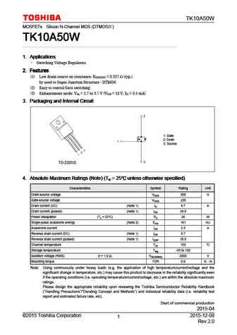
TK10A50W MOSFETs Silicon N-Channel MOS (DTMOS ) TK10A50W TK10A50W TK10A50W TK10A50W 1. Applications 1. Applications 1. Applications 1. Applications Switching Voltage Regulators 2. Features 2. Features 2. Features 2. Features (1) Low drain-source on-resistance RDS(ON) = 0.327 (typ.) by used to Super Junction Structure DTMOS (2) Easy to control Gate switching (3) E... See More ⇒
tk10a50w.pdf
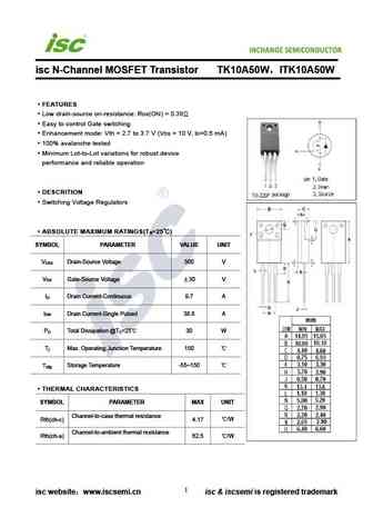
INCHANGE Semiconductor isc N-Channel MOSFET Transistor TK10A50W ITK10A50W FEATURES Low drain-source on-resistance RDS(ON) = 0.38 Easy to control Gate switching Enhancement mode Vth = 2.7 to 3.7 V (VDS = 10 V, ID=0.5 mA) 100% avalanche tested Minimum Lot-to-Lot variations for robust device performance and reliable operation DESCRITION Switching Voltage Regulators... See More ⇒
Detailed specifications: TJ50S06M3L, TJ60S04M3L, TJ60S06M3L, TJ70A06J3, TJ80S04M3L, TJ8S06M3L, TK100F04K3, TK100F06K3, 2N60, TK10A55D, TK10A60D, TK10S04K3L, TK10X40D, TK11A45D, TK11A50D, TK11A55D, TK11A60D
Keywords - TK10A50D MOSFET specs
TK10A50D cross reference
TK10A50D equivalent finder
TK10A50D pdf lookup
TK10A50D substitution
TK10A50D replacement
Learn how to find the right MOSFET substitute. A guide to cross-reference, check specs and replace MOSFETs in your circuits.
MOSFET Parameters. How They Affect Each Other
🌐 : EN ES РУ

LIST
Last Update
MOSFET: CB3139KTB | CB2301DW | BC8205 | BC3415 | BC3407 | BC3401 | BC3400 | BC2301 | BC1012W | BC1012T
Popular searches
jcs9n50fc datasheet | 2n2147 | 2sc870 | 2sa771 | d667 | a965 transistor | hy3210 | d313 transistor equivalent