CEM3301 Datasheet. Specs and Replacement
Type Designator: CEM3301 📄📄
Type of Transistor: MOSFET
Type of Control Channel: P-Channel
Absolute Maximum Ratings
Pd ⓘ - Maximum Power Dissipation: 2.5 W
|Vds|ⓘ - Maximum Drain-Source Voltage: 30 V
|Vgs|ⓘ - Maximum Gate-Source Voltage: 20 V
|Id| ⓘ - Maximum Drain Current: 7 A
Tj ⓘ - Maximum Junction Temperature: 150 °C
Electrical Characteristics
tr ⓘ - Rise Time: 6 nS
Cossⓘ - Output Capacitance: 220 pF
RDSonⓘ - Maximum Drain-Source On-State Resistance: 0.032 Ohm
Package: SO8
📄📄 Copy
CEM3301 substitution
- MOSFET ⓘ Cross-Reference Search
CEM3301 datasheet
cem3301.pdf

CEM3301 P-Channel Enhancement Mode Field Effect Transistor FEATURES -30V, -7.0A, RDS(ON) = 32m @VGS = -10V. RDS(ON) = 50m @VGS = -4.5V. Super high dense cell design for extremely low RDS(ON). High power and current handing capability. D D D D Lead free product is acquired. 8 7 6 5 Surface mount Package. SO-8 1 2 3 4 1 S S S G ABSOLUTE MAXIMUM RATINGS TA = 25 C unless othe... See More ⇒
cem3307.pdf
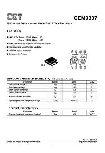
CEM3307 P-Channel Enhancement Mode Field Effect Transistor FEATURES -30V, -6.2A, RDS(ON) = 33m @VGS = -10V. RDS(ON) = 52m @VGS = -4.5V. Super high dense cell design for extremely low RDS(ON). High power and current handing capability. Lead free product is acquired. D1 D1 D2 D2 8 7 6 5 Surface mount Package. SO-8 1 2 3 4 1 S1 G1 S2 G2 ABSOLUTE MAXIMUM RATINGS TA = 25 C unles... See More ⇒
cem3307.pdf
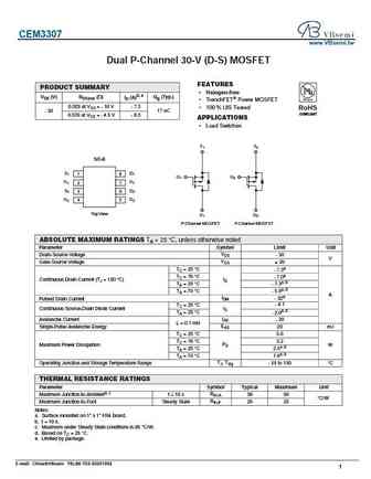
CEM3307 www.VBsemi.tw Dual P-Channel 30-V (D-S) MOSFET FEATURES PRODUCT SUMMARY Halogen-free VDS (V) RDS(on) ( ) ID (A)d, e Qg (Typ.) TrenchFET Power MOSFET 0.029 at VGS = - 10 V - 7.3 100 % UIS Tested RoHS - 30 17 nC COMPLIANT 0.039 at VGS = - 4.5 V - 6.3 APPLICATIONS Load Switches S1 S2 SO-8 S1 1 D1 8 G1 G2 G1 2 D1 7 S2 3 D2 6 G2 4 D2 5 Top View... See More ⇒
cem3317.pdf
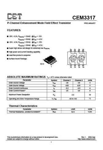
CEM3317 P-Channel Enhancement Mode Field Effect Transistor PRELIMINARY FEATURES -30V, -6.2A, RDS(ON) = 33m @VGS = -10V. RDS(ON) = 52m @VGS = -4.5V. -30V, -4.9A, RDS(ON) = 52m @VGS = -10V. RDS(ON) = 85m @VGS = -4.5V. Super high dense cell design for extremely low RDS(ON). D1 D1 D2 D2 8 7 6 5 High power and current handing capability. Lead free product is acquired. Surfa... See More ⇒
Detailed specifications: CEH3456, CEM2163, CEM2187, CEM2281, CEM2401, CEM2407, CEM3053, CEM3083, STF13NM60N, CEM3307, CEM3317, CEM3405L, CEM3407L, CEM4201, CEM4207, CEM4301, CEM4311
Keywords - CEM3301 MOSFET specs
CEM3301 cross reference
CEM3301 equivalent finder
CEM3301 pdf lookup
CEM3301 substitution
CEM3301 replacement
Can't find your MOSFET? Learn how to find a substitute transistor by analyzing voltage, current and package compatibility
MOSFET Parameters. How They Affect Each Other
🌐 : EN ES РУ

LIST
Last Update
MOSFET: BC2301 | BC1012W | BC1012T | BC1012 | 2SK3019WT | 2SK3019W | 2SK3018WT | CS95118 | CS85105A | CS75N45
Popular searches
hy3210 | d313 transistor equivalent | 2sb827 | c5200 datasheet | 2n2614 | 2sa777 replacement | 2sc828 transistor | 2sd357