CEU12P10 Datasheet. Specs and Replacement
Type Designator: CEU12P10 📄📄
Type of Transistor: MOSFET
Type of Control Channel: P-Channel
Absolute Maximum Ratings
Pd ⓘ - Maximum Power Dissipation: 50 W
|Vds|ⓘ - Maximum Drain-Source Voltage: 100 V
|Vgs|ⓘ - Maximum Gate-Source Voltage: 30 V
|Id| ⓘ - Maximum Drain Current: 9 A
Tj ⓘ - Maximum Junction Temperature: 150 °C
Electrical Characteristics
tr ⓘ - Rise Time: 7 nS
Cossⓘ - Output Capacitance: 115 pF
RDSonⓘ - Maximum Drain-Source On-State Resistance: 0.315 Ohm
Package: TO252
📄📄 Copy
CEU12P10 substitution
- MOSFET ⓘ Cross-Reference Search
CEU12P10 datasheet
ced12p10 ceu12p10.pdf
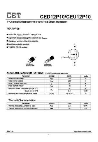
CED12P10/CEU12P10 P-Channel Enhancement Mode Field Effect Transistor FEATURES -100V, -9A, RDS(ON) = 315m @VGS = -10V. Super high dense cell design for extremely low RDS(ON). High power and current handing capability. Lead free product is acquired. D TO-251 & TO-252 package. D G G S CEU SERIES CED SERIES S TO-252(D-PAK) TO-251(I-PAK) ABSOLUTE MAXIMUM RATINGS Tc = 25 C unless ... See More ⇒
ceu12n10 ced12n10.pdf

CED12N10/CEU12N10 N-Channel Enhancement Mode Field Effect Transistor FEATURES 100V, 11A, RDS(ON) = 180m @VGS = 10V. Super high dense cell design for extremely low RDS(ON). High power and current handing capability. D Lead free product is acquired. TO-251 & TO-252 package. G D G S CEU SERIES CED SERIES S TO-252(D-PAK) TO-251(I-PAK) ABSOLUTE MAXIMUM RATINGS Tc = 25 C unless o... See More ⇒
ced12n10 ceu12n10.pdf
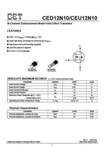
CED12N10/CEU12N10 N-Channel Enhancement Mode Field Effect Transistor FEATURES 100V, 11A, RDS(ON) = 180m @VGS = 10V. Super high dense cell design for extremely low RDS(ON). High power and current handing capability. D Lead free product is acquired. TO-251 & TO-252 package. G D G S CEU SERIES CED SERIES S TO-252(D-PAK) TO-251(I-PAK) ABSOLUTE MAXIMUM RATINGS Tc = 25 C unless o... See More ⇒
ceu12n10l ced12n10l.pdf
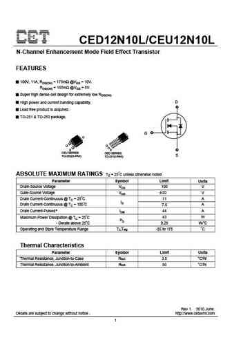
CED12N10L/CEU12N10L N-Channel Enhancement Mode Field Effect Transistor FEATURES 100V, 11A, RDS(ON) = 175m @VGS = 10V. RDS(ON) = 185m @VGS = 5V. Super high dense cell design for extremely low RDS(ON). High power and current handing capability. D Lead free product is acquired. TO-251 & TO-252 package. G D G S CEU SERIES CED SERIES S TO-252(D-PAK) TO-251(I-PAK) ABSOLUTE MA... See More ⇒
Detailed specifications: CES2331, CET4301, CET4435A, CET6601, CET6861, CET9435A, CEU05P03, CEU11P20, IRFB4227, CEU20P06, CEU20P10, CEU2303, CEU30P10, CEU3301, CEU3423, CEU4201, CEU4301
Keywords - CEU12P10 MOSFET specs
CEU12P10 cross reference
CEU12P10 equivalent finder
CEU12P10 pdf lookup
CEU12P10 substitution
CEU12P10 replacement
Can't find your MOSFET? Learn how to find a substitute transistor by analyzing voltage, current and package compatibility
MOSFET Parameters. How They Affect Each Other
History: BRCS200N10SZC | APG082N01 | CS4N65A3HDY | CSD19533KCS | KF5N53D | FS50KMJ-06F | IXFK180N25T
🌐 : EN ES РУ

LIST
Last Update
MOSFET: CS95118 | CS85105A | CS75N45 | CS72N12 | CS55N50 | CS48N75A | CS40N27 | MSQ60P04D | MSQ40P07D | MSQ30P40D
Popular searches
2sd1047 transistor | mj802 | bu508a | bc560c | ksa1220ay | irf 830 | mpsa56 transistor | transistor 2222a