NDD60N550U1 Datasheet. Specs and Replacement
Type Designator: NDD60N550U1 📄📄
Type of Transistor: MOSFET
Type of Control Channel: N-Channel
Absolute Maximum Ratings
Pd ⓘ - Maximum Power Dissipation: 94 W
|Vds|ⓘ - Maximum Drain-Source Voltage: 600 V
|Vgs|ⓘ - Maximum Gate-Source Voltage: 25 V
|Id| ⓘ - Maximum Drain Current: 8.2 A
Tj ⓘ - Maximum Junction Temperature: 150 °C
Electrical Characteristics
tr ⓘ - Rise Time: 14 nS
Cossⓘ - Output Capacitance: 33 pF
📄📄 Copy
NDD60N550U1 substitution
- MOSFET ⓘ Cross-Reference Search
NDD60N550U1 datasheet
ndd60n550u1.pdf
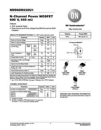
NDD60N550U1 N-Channel Power MOSFET 600 V, 550 mW Features 100% Avalanche Tested These Devices are Pb-Free, Halogen Free/BFR Free and are RoHS http //onsemi.com Compliant V(BR)DSS RDS(ON) MAX ABSOLUTE MAXIMUM RATINGS (TJ = 25 C unless otherwise noted) 600 V 550 mW @ 10 V Parameter Symbol NDD Unit Drain-to-Source Voltage VDSS 600 V Gate-to-Source Voltage VGS 25 V N-Channel... See More ⇒
ndd60n360u1.pdf
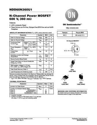
NDD60N360U1 N-Channel Power MOSFET 600 V, 360 mW Features 100% Avalanche Tested These Devices are Pb-Free, Halogen Free/BFR Free and are RoHS http //onsemi.com Compliant V(BR)DSS RDS(ON) MAX ABSOLUTE MAXIMUM RATINGS (TJ = 25 C unless otherwise noted) Parameter Symbol NDD Unit 600 V 360 mW @ 10 V Drain-to-Source Voltage VDSS 600 V Gate-to-Source Voltage VGS 25 V N-Channel... See More ⇒
ndd60n900u1.pdf
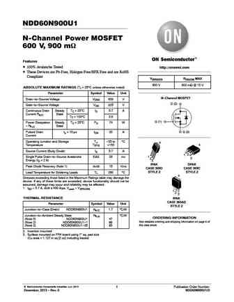
NDD60N900U1 N-Channel Power MOSFET 600 V, 900 mW Features 100% Avalanche Tested http //onsemi.com These Devices are Pb-Free, Halogen Free/BFR Free and are RoHS Compliant V(BR)DSS RDS(ON) MAX 600 V 900 mW @ 10 V ABSOLUTE MAXIMUM RATINGS (TJ = 25 C unless otherwise noted) Parameter Symbol Value Unit N-Channel MOSFET Drain-to-Source Voltage VDSS 600 V D (2) Gate-to-Source V... See More ⇒
ndd60n745u1.pdf
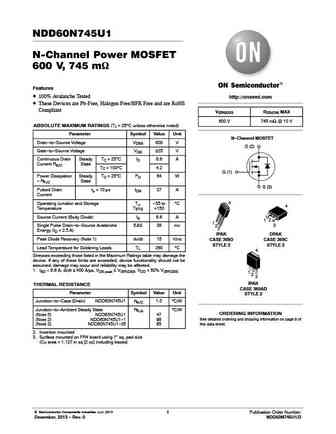
NDD60N745U1 N-Channel Power MOSFET 600 V, 745 mW Features 100% Avalanche Tested http //onsemi.com These Devices are Pb-Free, Halogen Free/BFR Free and are RoHS Compliant V(BR)DSS RDS(ON) MAX 600 V 745 mW @ 10 V ABSOLUTE MAXIMUM RATINGS (TJ = 25 C unless otherwise noted) Parameter Symbol Value Unit N-Channel MOSFET Drain-to-Source Voltage VDSS 600 V D (2) Gate-to-Source V... See More ⇒
Detailed specifications: NDBA100N10B, NDBA170N06A, NDBA180N10B, NDD01N60, NDD02N40, NDD03N40Z, NDD03N80Z, NDD60N360U1, AON7410, NDD60N745U1, NDD60N900U1, NDDL01N60Z, NDDP010N25AZ, NDFP03N150C, NDFP03N150CG, NDFPD1N150C, NDFPD1N150CG
Keywords - NDD60N550U1 MOSFET specs
NDD60N550U1 cross reference
NDD60N550U1 equivalent finder
NDD60N550U1 pdf lookup
NDD60N550U1 substitution
NDD60N550U1 replacement
Can't find your MOSFET? Learn how to find a substitute transistor by analyzing voltage, current and package compatibility
MOSFET Parameters. How They Affect Each Other
History: SI7434DP | SI7456DDP | IXFK120N30T | MTP4N08 | SI7446BDP | 2SK4066 | APT60M75L2LLG
🌐 : EN ES РУ

LIST
Last Update
MOSFET: CS95118 | CS85105A | CS75N45 | CS72N12 | CS55N50 | CS48N75A | CS40N27 | MSQ60P04D | MSQ40P07D | MSQ30P40D
Popular searches
c711 transistor | k3599 transistor datasheet | 2sc1735 | transistor 2sc5200 | 2sb560 transistor | a1273 | c3421 transistor | c644 transistor