PB502CW Datasheet. Specs and Replacement
Type Designator: PB502CW 📄📄
Type of Transistor: MOSFET
Type of Control Channel: NP-Channel
Absolute Maximum Ratings
Pd ⓘ - Maximum Power Dissipation: 1.9 W
|Vds|ⓘ - Maximum Drain-Source Voltage: 20 V
|Vgs|ⓘ - Maximum Gate-Source Voltage: 8 V
|Id| ⓘ - Maximum Drain Current: 3.8 A
Tj ⓘ - Maximum Junction Temperature: 150 °C
Electrical Characteristics
tr ⓘ - Rise Time: 33 nS
Cossⓘ - Output Capacitance: 82 pF
RDSonⓘ - Maximum Drain-Source On-State Resistance: 0.03 Ohm
Package: PDFN2X2S
📄📄 Copy
PB502CW substitution
- MOSFET ⓘ Cross-Reference Search
PB502CW datasheet
pb502cw.pdf
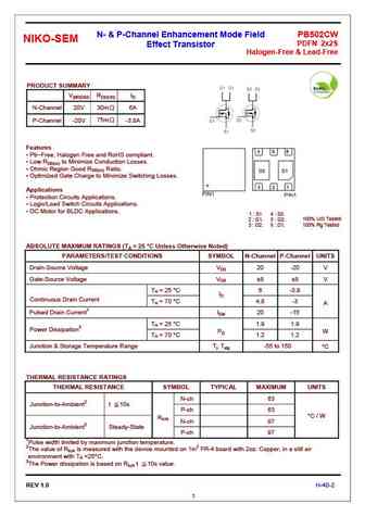
N- & P-Channel Enhancement Mode Field PB502CW NIKO-SEM PDFN 2x2S Effect Transistor Halogen-Free & Lead-Free PRODUCT SUMMARY V(BR)DSS RDS(ON) ID N-Channel 20V 30m 6A P-Channel -20V 75m -3.8A Features Pb-Free, Halogen Free and RoHS compliant. Low RDS(on) to Minimize Conduction Losses. Ohmic Region Good RDS(on) Ratio. Optimized Gate Charge to Minimize... See More ⇒
Detailed specifications: PA5D8EA, PA5D8JA, PA5S6EA, PA5S6JA, PA607UA, PA710ED, PA910BC, PA910BM, 13N50, PB5A2BX, PB5A3JW, PB5B5BX, PB5C5JW, PB5G8JW, PB600BX, PB606BX, PB6C4JU
Keywords - PB502CW MOSFET specs
PB502CW cross reference
PB502CW equivalent finder
PB502CW pdf lookup
PB502CW substitution
PB502CW replacement
Can't find your MOSFET? Learn how to find a substitute transistor by analyzing voltage, current and package compatibility
MOSFET Parameters. How They Affect Each Other
🌐 : EN ES РУ

LIST
Last Update
MOSFET: CS95118 | CS85105A | CS75N45 | CS72N12 | CS55N50 | CS48N75A | CS40N27 | MSQ60P04D | MSQ40P07D | MSQ30P40D
Popular searches
2sb647 | k3561 transistor | c3203 transistor | irfp450 equivalent | 2sb649 | 2sb324 transistor | b754 transistor | 2sc828 equivalent