1402 Datasheet. Specs and Replacement
Type Designator: 1402 📄📄
Material of Transistor: Si
Polarity: NPN
Absolute Maximum Ratings
Maximum Collector Power Dissipation (Pc): 0.6 W
Maximum Collector-Base Voltage |Vcb|: 35 V
Maximum Collector-Emitter Voltage |Vce|: 30 V
Maximum Emitter-Base Voltage |Veb|: 4 V
Maximum Collector Current |Ic max|: 0.05 A
Max. Operating Junction Temperature (Tj): 150 °C
Electrical Characteristics
Forward Current Transfer Ratio (hFE), MIN: 110
Noise Figure, dB: -
Package: TO92
📄📄 Copy
- BJT ⓘ Cross-Reference Search
1402 datasheet
0.1. Size:41K st
msc81402.pdf 
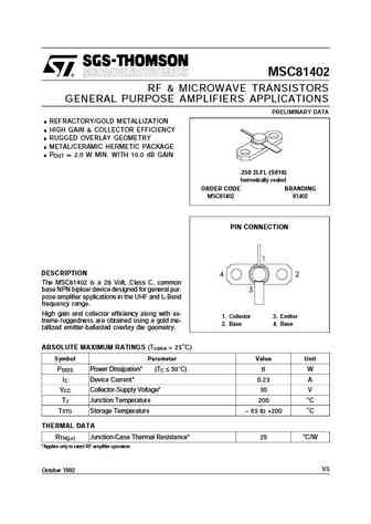
MSC81402 RF & MICROWAVE TRANSISTORS GENERAL PURPOSE AMPLIFIERS APPLICATIONS PRELIMINARY DATA .REFRACTORY/GOLD METALLIZATION .HIGH GAIN & COLLECTOR EFFICIENCY .RUGGED OVERLAY GEOMETRY .METAL/CERAMIC HERMETIC PACKAGE .P 2.0 W MIN. WITH 10.0 dB GAIN = OUT .250 2LFL (S010) hermetically sealed ORDER CODE BRANDING MSC81402 81402 PIN CONNECTION DESCRIPTION The MSC81402 is a 28 Volt, C... See More ⇒
0.2. Size:580K toshiba
rn1401 rn1402 rn1403 rn1404 rn1405 rn1406.pdf
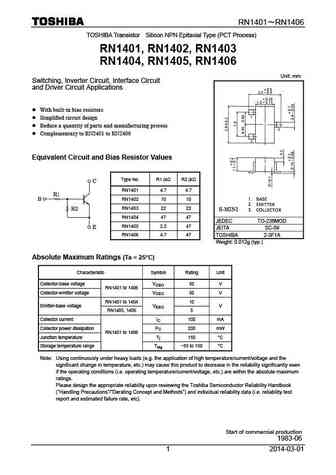
RN1401 RN1406 TOSHIBA Transistor Silicon NPN Epitaxial Type (PCT Process) RN1401, RN1402, RN1403 RN1404, RN1405, RN1406 Unit mm Switching, Inverter Circuit, Interface Circuit and Driver Circuit Applications With built-in bias resistors Simplified circuit design Reduce a quantity of parts and manufacturing process Complementary to RN2401 to RN2406 Equivalent Cir... See More ⇒
0.3. Size:118K sanyo
2sa1402 2sc3596.pdf
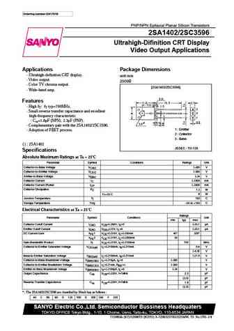
Ordering number EN1761B PNP/NPN Epitaxial Planar Silicon Transistors 2SA1402/2SC3596 Ultrahigh-Difinition CRT Display Video Output Applications Applications Package Dimensions Ultrahigh-definition CRT display. unit mm Video output. 2009B Color TV chroma output. [2SA1402/2SC3596] Wide-band amp. Features High fT fT typ=700MHz. Small reverse transfer capacit... See More ⇒
0.4. Size:82K renesas
2sk1402.pdf
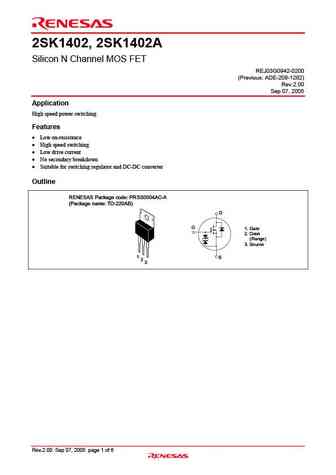
2SK1402, 2SK1402A Silicon N Channel MOS FET REJ03G0942-0200 (Previous ADE-208-1282) Rev.2.00 Sep 07, 2005 Application High speed power switching Features Low on-resistance High speed switching Low drive current No secondary breakdown Suitable for switching regulator and DC-DC converter Outline RENESAS Package code PRSS0004AC-A (Package name ... See More ⇒
0.5. Size:94K vishay
si1402dh.pdf
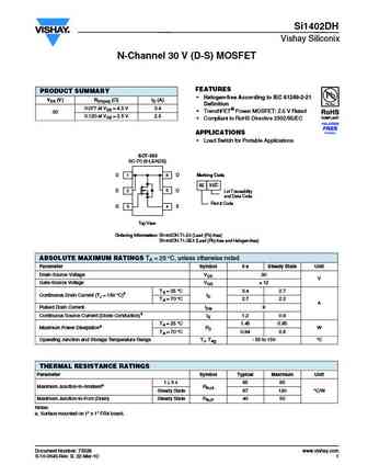
Si1402DH Vishay Siliconix N-Channel 30 V (D-S) MOSFET FEATURES PRODUCT SUMMARY Halogen-free According to IEC 61249-2-21 VDS (V) RDS(on) ( )ID (A) Definition 0.077 at VGS = 4.5 V 3.4 TrenchFET Power MOSFET 2.5 V Rated 30 0.120 at VGS = 2.5 V 2.5 Compliant to RoHS Directive 2002/95/EC APPLICATIONS Load Switch for Portable Applications SOT-363 SC-70 (6-LEA... See More ⇒
0.6. Size:614K infineon
ptfb241402f.pdf
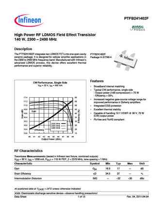
PTFB241402F Confidential, Limited Internal Distribution High Power RF LDMOS Field Effect Transistor 140 W, 2300 2400 MHz Description The PTFB241402F integrates two LDMOS FETs into one open-cavity PTFB241402F ceramic package. It is designed for cellular amplifier applications in Package H-37248-4 the 2300 to 2400 MHz frequency band. Manufactured with Infineon s advanced LDMO... See More ⇒
0.7. Size:478K onsemi
pcp1402.pdf
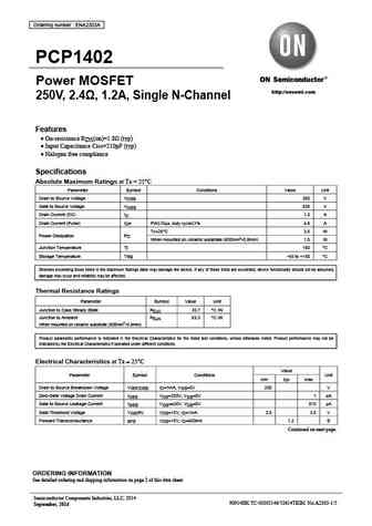
Ordering number ENA2303A PCP1402 Power MOSFET http //onsemi.com 250V, 2.4 , 1.2A, Single N-Channel Features On-resistance RDS(on)=1.8 (typ) Input Capacitance Ciss=210pF (typ) Halogen free compliance Specifications Absolute Maximum Ratings at Ta = 25 C Parameter Symbol Conditions Value Unit Drain to Source Voltage VDSS 250 V Gate to Source Voltage VG... See More ⇒
0.8. Size:104K savantic
2sc1402.pdf
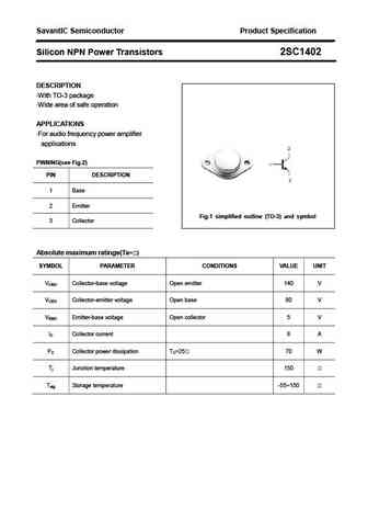
SavantIC Semiconductor Product Specification Silicon NPN Power Transistors 2SC1402 DESCRIPTION With TO-3 package Wide area of safe operation APPLICATIONS For audio frequency power amplifier applications PINNING(see Fig.2) PIN DESCRIPTION 1 Base 2 Emitter Fig.1 simplified outline (TO-3) and symbol 3 Collector Absolute maximum ratings(Ta= ) SYMBOL PARAMETER CONDI... See More ⇒
0.9. Size:68K wingshing
2sd1402.pdf
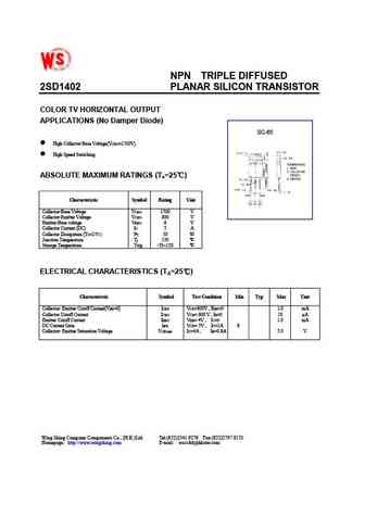
NPN TRIPLE DIFFUSED 2SD1402 PLANAR SILICON TRANSISTOR COLOR TV HORIZONTAL OUTPUT APPLICATIONS (No Damper Diode) SC-65 High Collector-Base Voltage(VCBO=1500V) High Speed Switching ABSOLUTE MAXIMUM RATINGS (T =25 ) A Characteristic Symbol Rating Unit Collector-Base Voltage VCBO 1500 V Collector-Emitter Voltage VCEO 800 V Emitter-Base voltage VEBO 6 V Collecto... See More ⇒
0.10. Size:2223K goford
1402tr.pdf
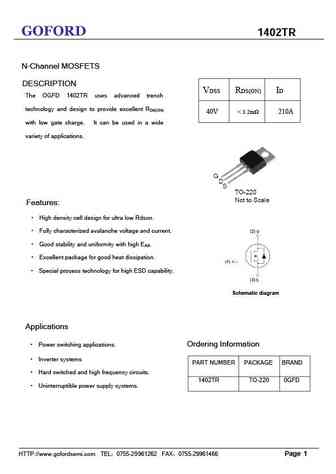
GOFORD 1402TR N-Channel MOSFETS DESCRIPTION VDSS RDS(ON) ID The OGFD 1402TR uses advanced trench technology and design to provide excellent R DS(ON) 40V ... See More ⇒
0.11. Size:548K unikc
p1402cdg.pdf
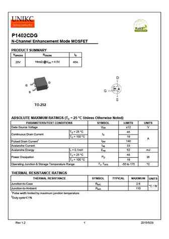
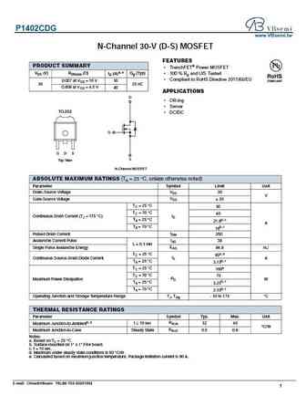
P1402CDG N-Channel Enhancement Mode MOSFET PRODUCT SUMMARY V(BR)DSS RDS(ON) ID 14m @VGS = 4.5V 20V 45A TO-252 ABSOLUTE MAXIMUM RATINGS (TC = 25 C Unless Otherwise Noted) PARAMETERS/TEST CONDITIONS SYMBOL LIMITS UNITS VGS Gate-Source Voltage 12 V TC = 25 C 45 ID Continuous Drain Current TC = 100 C 19 A IDM 140 Pulsed Drain Current1 IAS Avalanche Current 33 ... See More ⇒
0.12. Size:162K sino
sm1402nss.pdf
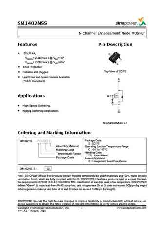
SM1402NSS N-Channel Enhancement Mode MOSFET Features Pin Description 60V/0.4A, D RDS(ON)= 2.2 (max.) @ VGS=10V S RDS(ON)= 2.6 (max.) @ VGS=4.5V G ESD Protection Top View of SC-70 Reliable and Rugged Lead Free and Green Devices Available D (RoHS Compliant) G Applications High Speed Switching. Analog Switching Application. S N-Channel MOSFET Ordering and Ma... See More ⇒
0.13. Size:1057K magnachip
mdu1402vrh.pdf
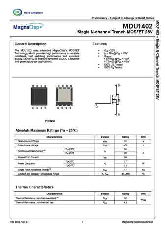
Preliminary Subject to Change without Notice MDU1402 Single N-channel Trench MOSFET 25V General Description Features The MDU1402 uses advanced MagnaChip s MOSFET V = 25V DS Technology, which provides high performance in on-state I = 66A @V = 10V D GS resistance, fast switching performance and excellent R DS(ON) quality. MDU1402 is suitable device for DC/DC... See More ⇒
0.14. Size:1306K elm
elm51402fa.pdf
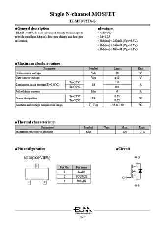
Single N-channel MOSFET ELM51402FA-S General description Features ELM51402FA-S uses advanced trench technology to Vds=20V provide excellent Rds(on), low gate charge and low gate Id=1.0A resistance. Rds(on) ... See More ⇒
0.15. Size:91K sensitron
sff914028.pdf
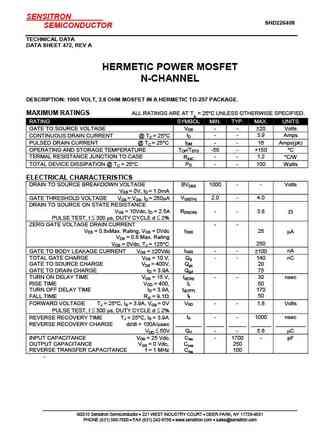
SENSITRON SHD226408 SEMICONDUCTOR TECHNICAL DATA DATA SHEET 472, REV A HERMETIC POWER MOSFET N-CHANNEL DESCRIPTION 1000 VOLT, 3.8 OHM MOSFET IN A HERMETIC TO-257 PACKAGE. MAXIMUM RATINGS ALL RATINGS ARE AT TA = 25 C UNLESS OTHERWISE SPECIFIED. RATING SYMBOL MIN. TYP. MAX. UNITS GATE TO SOURCE VOLTAGE VGS - - Volts 20 ID - - 3.9 Amps CONTINUOUS DRAIN CURRENT @ TC... See More ⇒
0.16. Size:843K cn vbsemi
p1402cdg.pdf
P1402CDG www.VBsemi.tw N-Channel 30-V (D-S) MOSFET FEATURES PRODUCT SUMMARY TrenchFET Power MOSFET VDS (V) RDS(on) ( ) ID (A)a, e Qg (Typ) 100 % Rg and UIS Tested Compliant to RoHS Directive 2011/65/EU 0.007 at VGS = 10 V 50 30 25 nC 0.009 at VGS = 4.5 V 40 APPLICATIONS D OR-ing Server TO-252 DC/DC G G D S S Top View N-Channel MOSFET ABSOL... See More ⇒
0.17. Size:935K cn vbsemi
vbqa1402.pdf
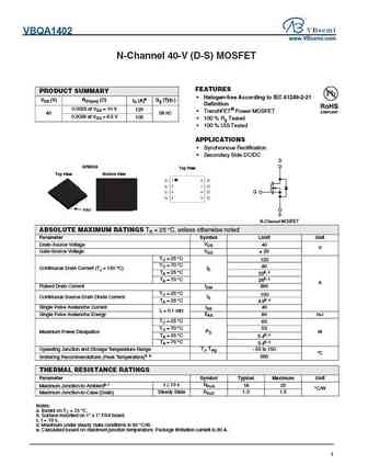
VBQA1402 www.VBsemi.com N-Channel 40-V (D-S) MOSFET FEATURES PRODUCT SUMMARY Halogen-free According to IEC 61249-2-21 VDS (V) RDS(on) ( ) ID (A)a Qg (Typ.) Definition 0.0025 at VGS = 10 V 120 TrenchFET Power MOSFET 40 38 nC 0.0028 at VGS = 6.5 V 105 100 % Rg Tested 100 % UIS Tested APPLICATIONS Synchronous Rectification Secondary Side DC/DC... See More ⇒
0.18. Size:635K cn vbsemi
vbm1402.pdf
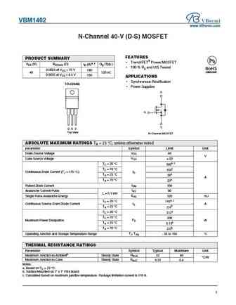
VBM1402 www.VBsemi.com N-Channel 40-V (D-S) MOSFET FEATURES PRODUCT SUMMARY TrenchFET Power MOSFET VDS (V) RDS(on) ( ) ID (A)a, c Qg (Typ.) 100 % Rg and UIS Tested RoHS 0.0024 at VGS = 10 V 180 COMPLIANT 40 120 nC 0.0035 at VGS = 6.5 V 150 APPLICATIONS Synchronous Rectification TO-220AB Power Supplies D G S G D S Top View N-Channel MOSFET ABSOLUT... See More ⇒
0.19. Size:217K inchange semiconductor
2sd1402.pdf
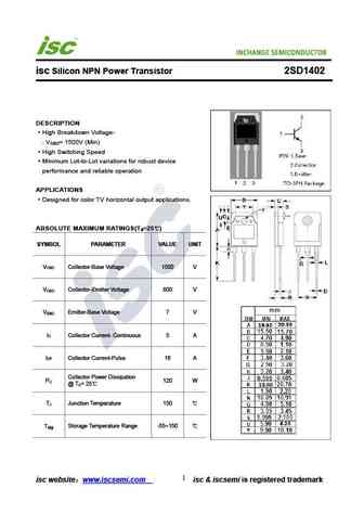
isc Silicon NPN Power Transistor 2SD1402 DESCRIPTION High Breakdown Voltage- V = 1500V (Min) CBO High Switching Speed Minimum Lot-to-Lot variations for robust device performance and reliable operation APPLICATIONS Designed for color TV horizontal output applications. ABSOLUTE MAXIMUM RATINGS(T =25 ) a SYMBOL PARAMETER VALUE UNIT V Collector-Base Voltage 1500 V CBO V C... See More ⇒
0.20. Size:199K inchange semiconductor
2sk1402a.pdf
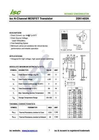
isc N-Channel MOSFET Transistor 2SK1402A DESCRIPTION Drain Current I = 4A@ T =25 D C Drain Source Voltage- V = 650V(Min) DSS Fast Switching Speed Minimum Lot-to-Lot variations for robust device performance and reliable operation APPLICATIONS Designed for high voltage, high speed power switching ABSOLUTE MAXIMUM RATINGS(T =25 ) a SYMBOL ARAMETER VALUE UNIT V Dr... See More ⇒
0.21. Size:214K inchange semiconductor
2sb1402.pdf
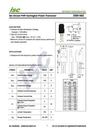
isc Silicon PNP Darlington Power Transistor 2SB1402 DESCRIPTION Collector-Emitter Breakdown Voltage- V = -120V(Min) (BR)CEO High DC Current Gain- h = 1000(Min)@ (V = -3V, I = -1.5A) FE CE C Minimum Lot-to-Lot variations for robust device performance and reliable operation APPLICATIONS Designed for low frequency power amplifier applications. ABSOLUTE MAXIMUM RATINGS(T =25... See More ⇒
0.22. Size:102K inchange semiconductor
2sc1402.pdf

SavantIC Semiconductor Product Specification Silicon NPN Power Transistors 2SC1402 DESCRIPTION With TO-3 package Wide area of safe operation APPLICATIONS For audio frequency power amplifier applications PINNING(see Fig.2) PIN DESCRIPTION 1 Base 2 Emitter Fig.1 simplified outline (TO-3) and symbol 3 Collector Absolute maximum ratings(Ta= ) SYMBOL PARAMETER CONDI... See More ⇒
0.23. Size:199K inchange semiconductor
2sk1402.pdf
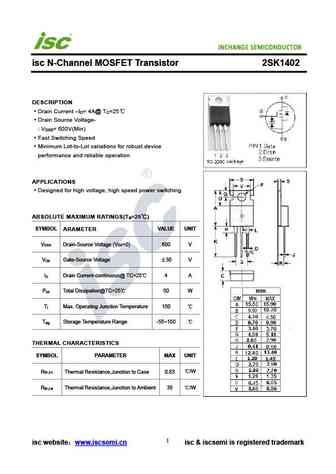
isc N-Channel MOSFET Transistor 2SK1402 DESCRIPTION Drain Current I = 4A@ T =25 D C Drain Source Voltage- V = 600V(Min) DSS Fast Switching Speed Minimum Lot-to-Lot variations for robust device performance and reliable operation APPLICATIONS Designed for high voltage, high speed power switching ABSOLUTE MAXIMUM RATINGS(T =25 ) a SYMBOL ARAMETER VALUE UNIT V Dra... See More ⇒
Detailed specifications: 121-477, 121-695, 121-713, 121-744, 121-746, 121-755, 121-792, 1401, 13003, 142T2, 1501, 1502, 152NU70, 153NU70, 154NU70, 155NU70, 1601
Keywords - 1402 pdf specs
1402 cross reference
1402 equivalent finder
1402 pdf lookup
1402 substitution
1402 replacement
