R340 Datasheet. Specs and Replacement
Type Designator: R340 📄📄
Material of Transistor: Si
Polarity: NPN
Absolute Maximum Ratings
Maximum Collector Power Dissipation (Pc): 0.36 W
Maximum Collector-Base Voltage |Vcb|: 40 V
Maximum Collector-Emitter Voltage |Vce|: 30 V
Maximum Emitter-Base Voltage |Veb|: 5 V
Maximum Collector Current |Ic max|: 0.5 A
Max. Operating Junction Temperature (Tj): 150 °C
Electrical Characteristics
Transition Frequency (ft): 250 MHz
Collector Capacitance (Cc): 8 pF
Forward Current Transfer Ratio (hFE), MIN: 60
Noise Figure, dB: -
📄📄 Copy
- BJT ⓘ Cross-Reference Search
R340 datasheet
0.1. Size:253K infineon
ipi90r340c3.pdf 

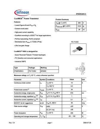
IPI90R340C3 CoolMOS Power Transistor Product Summary Features V @ T =25 C 900 V DS J Lowest figure-of-merit RON x Qg R @T =25 C 0.34 DS(on),max J Extreme dv/dt rated Q 94 nC g,typ High peak current capability Qualified according to JEDEC1) for target applications Pb-free lead plating; RoHS compliant Worldwide best R in TO262 (I2Pak) PG-TO262 DS... See More ⇒
0.2. Size:637K infineon
ipw90r340c3.pdf 

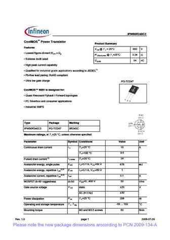
IPW90R340C3 C IMOS # A0IN U . J6A>;> 9 for industrial grade applications 688DG9>CC6CI U 2 AIG6 ADL ... See More ⇒
0.3. Size:267K infineon
ipa90r340c3.pdf 

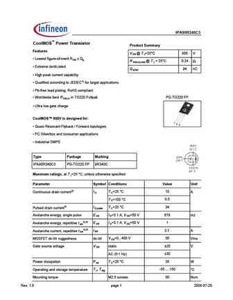
IPA90R340C3 CoolMOS Power Transistor Product Summary Features V @ T =25 C 900 V DS J Lowest figure-of-merit RON x Qg R @ T = 25 C 0.34 DS(on),max J Extreme dv/dt rated Q 94 nC g,typ High peak current capability Qualified according to JEDEC1) for target applications Pb-free lead plating; RoHS compliant Worldwide best R in TO220 Fullpak PG-TO220 FP... See More ⇒
0.4. Size:911K infineon
ipb90r340c3.pdf 

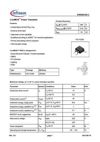
IPB90R340C3 CoolMOS Power Transistor Product Summary Features VDS @ TJ=25 C 900 V Lowest figure-of-merit RON x Qg RDS(on),max @TJ=25 C 0.34 W Extreme dv/dt rated Qg,typ 94 nC High peak current capability Qualified according to JEDEC1) for industrial applications PG-TO263 Pb-free lead plating; RoHS compliant Ultra low gate charge CoolMOS 900V is desi... See More ⇒
0.5. Size:1798K infineon
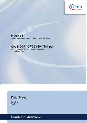
ipl65r340cfd.pdf 

MOSFET Metal Oxide Semiconductor Field Effect Transistor CoolMOS CFD2 650V Thinpak 650V CoolMOS CFD2 Power Transistor IPL65R340CFD Data Sheet Rev. 2.0 Final Industrial & Multimarket 650V CoolMOS CFD2 Power Transistor IPL65R340CFD ThinPAK 8x8 1 Description CoolMOS is a revolutionary technology for high voltage power MOSFETs, designed according to the superjunction (SJ... See More ⇒
0.6. Size:286K infineon
ipp90r340c3.pdf 

IPP90R340C3 CoolMOS Power Transistor Product Summary Features V @ T =25 C 900 V DS J Lowest figure-of-merit RON x Qg R @T =25 C 0.34 DS(on),max J Extreme dv/dt rated Q 94 nC g,typ High peak current capability Qualified according to JEDEC1) for target applications Pb-free lead plating; RoHS compliant PG-TO220 Worldwide best R in TO220 DS,on ... See More ⇒
0.15. Size:1169K sanrise-tech
src65r340ec.pdf 

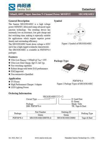
Datasheet 340m , 600V, Super Junction N-Channel Power MOSFET SRC65R340EC General Description Symbol The Sanrise SRC65R340EC is a high voltage power MOSFET, fabricated using advanced super junction technology. The resulting device has extremely low on resistance, low gate charge and fast switching time, making it especially suitable for applications which require superior power density... See More ⇒
0.16. Size:757K cn salltech
sr3401.pdf 

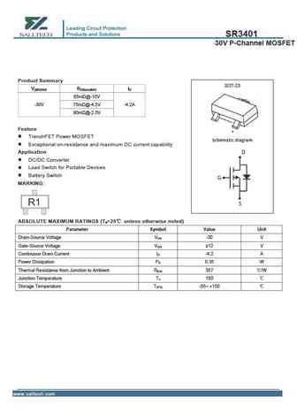
Leading Circuit Protection Products and Solutions SR3401 30V P-Channel MOSFET Product Summary SOT-23 V(BR)DSS RDS(on)MAX ID 65m @-10V D -30V 75m @-4.5V -4.2A 90m @-2.5V G Feature S TrenchFET Power MOSFET Schematic diagram Exceptional on-resistance and maximum DC current capability Application D DC/DC Converter Load Switch for Portable Devices Battery S... See More ⇒
0.17. Size:692K cn salltech
sr3400.pdf 

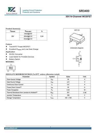
Leading Circuit Protection SR3400 Products and Solutions 30V N-Channel MOSFET Product Summary SOT-23 V R I (BR)DSS DS(on)MAX D 35m @10V 30V 40m @4.5V 5.8A 52m @2.5V Feature TrenchFET Power MOSFET Schematic diagram Excellent RDS(on) and Low Gate Charge Application DC/DC Converter Load Switch for Portable Devices Battery Switch MARKING ABSOLUTE MAXIMUM ... See More ⇒
0.18. Size:243K inchange semiconductor
ipw90r340c3.pdf 
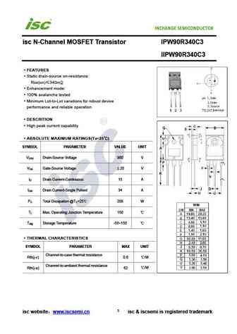
isc N-Channel MOSFET Transistor IPW90R340C3 IIPW90R340C3 FEATURES Static drain-source on-resistance RDS(on) 340m Enhancement mode 100% avalanche tested Minimum Lot-to-Lot variations for robust device performance and reliable operation DESCRITION High peak current capability ABSOLUTE MAXIMUM RATINGS(T =25 ) a SYMBOL PARAMETER VALUE UNIT V Drain-Source Volta... See More ⇒
0.19. Size:225K inchange semiconductor
ipa90r340c3.pdf 
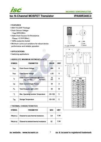
INCHANGE Semiconductor Isc N-Channel MOSFET Transistor IPA90R340C3 FEATURES With TO-220F Package Drain Source Voltage- V =900V(Min) DSS Static Drain-Source On-Resistance R = 0.34 (Max) DS(on) 100% avalanche tested Minimum Lot-to-Lot variations for robust device performance and reliable operation APPLICATIONS Switching applications ABSOLUTE MAXIMUM RATINGS(T... See More ⇒
0.20. Size:258K inchange semiconductor
ipb90r340c3.pdf 
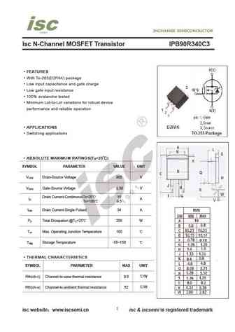
Isc N-Channel MOSFET Transistor IPB90R340C3 FEATURES With To-263(D2PAK) package Low input capacitance and gate charge Low gate input resistance 100% avalanche tested Minimum Lot-to-Lot variations for robust device performance and reliable operation APPLICATIONS Switching applications ABSOLUTE MAXIMUM RATINGS(T =25 ) a SYMBOL PARAMETER VALUE UNIT V Drain-Source V... See More ⇒
0.21. Size:245K inchange semiconductor
ipp90r340c3.pdf 
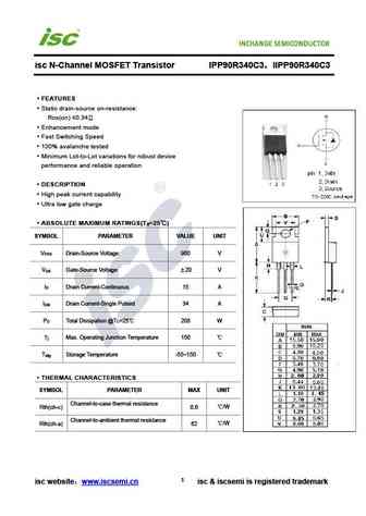
isc N-Channel MOSFET Transistor IPP90R340C3 IIPP90R340C3 FEATURES Static drain-source on-resistance RDS(on) 0.34 Enhancement mode Fast Switching Speed 100% avalanche tested Minimum Lot-to-Lot variations for robust device performance and reliable operation DESCRIPTION High peak current capability Ultra low gate charge ABSOLUTE MAXIMUM RATINGS(T =25 ) a... See More ⇒
0.22. Size:1551K cn apm
apj30n65f apj30n65p apj30n65t ap65r340.pdf 

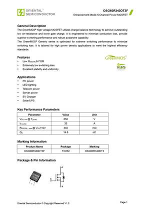
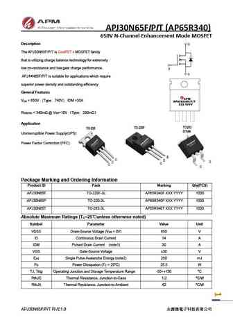
APJ30N65FIPIT (AP65R340) 650V N-Channel Enhancement Mode MOSFET Description The APJ30N65F/P/T is CoolFET II MOSFET family that is utilizing charge balance technology for extremely low on-resistance and low gate charge performance. APJ14N65F/P/T is suitable for applications which require superior power density and outstanding efficiency General Features V = 650V Type 740V... See More ⇒
Detailed specifications: Q-01169C, Q-05115C, Q-15115C, Q-36A, Q5077A, Q5102, Q-591-8003, R3283, 2SC5198, R3608-1, R582, R7249, R7360, R7887, R8066, R8070, R8118
Keywords - R340 pdf specs
R340 cross reference
R340 equivalent finder
R340 pdf lookup
R340 substitution
R340 replacement
