2N5643 Datasheet. Specs and Replacement
Type Designator: 2N5643 📄📄
Material of Transistor: Si
Polarity: NPN
Absolute Maximum Ratings
Maximum Collector Power Dissipation (Pc): 40 W
Maximum Collector-Base Voltage |Vcb|: 65 V
Maximum Collector-Emitter Voltage |Vce|: 35 V
Maximum Emitter-Base Voltage |Veb|: 4 V
Maximum Collector Current |Ic max|: 5 A
Max. Operating Junction Temperature (Tj): 200 °C
Electrical Characteristics
Transition Frequency (ft): 175 MHz
Collector Capacitance (Cc): 65 pF
Forward Current Transfer Ratio (hFE), MIN: 5
Package: TO128
📄📄 Copy
2N5643 Substitution
- BJT ⓘ Cross-Reference Search
2N5643 datasheet
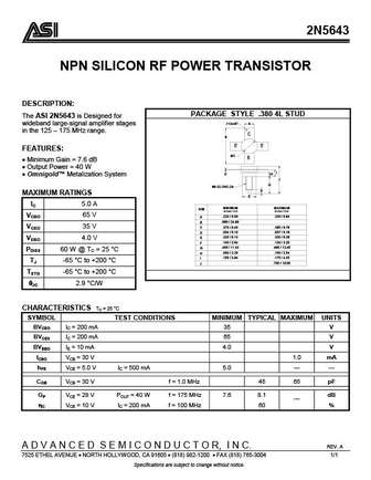
2N5643 NPN SILICON RF POWER TRANSISTOR DESCRIPTION PACKAGE STYLE .380 4L STUD The ASI 2N5643 is Designed for .112x45 A wideband large-signal amplifier stages in the 125 175 MHz range. C B E E FEATURES C B Minimum Gain = 7.6 dB Output Power = 40 W I D H Omnigold Metalization System J G #8-32 UNC-2A F MAXIMUM RATINGS E IC 5.0... See More ⇒
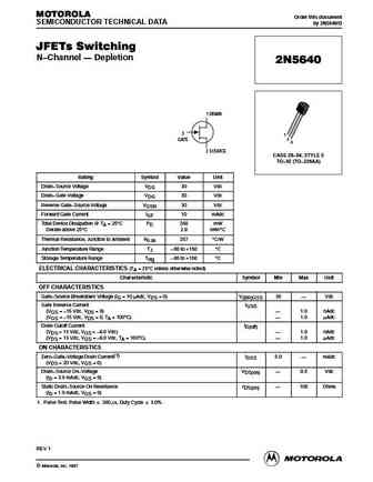
MOTOROLA Order this document SEMICONDUCTOR TECHNICAL DATA by 2N5640/D JFETs Switching N Channel Depletion 2N5640 1 DRAIN 3 1 GATE 2 3 2 SOURCE CASE 29 04, STYLE 5 TO 92 (TO 226AA) Rating Symbol Value Unit Drain Source Voltage VDS 30 Vdc Drain Gate Voltage VDG 30 Vdc Reverse Gate Source Voltage VGSR 30 Vdc Forward Gate Current IGF 10 mAdc Total Device Dissip... See More ⇒
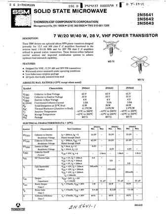
Detailed specifications: 2N5633, 2N5634, 2N5635, 2N5636, 2N5637, 2N564, 2N5641, 2N5642, 8050, 2N5644, 2N5645, 2N5646, 2N565, 2N5650, 2N5651, 2N5652, 2N5655
Keywords - 2N5643 pdf specs
2N5643 cross reference
2N5643 equivalent finder
2N5643 pdf lookup
2N5643 substitution
2N5643 replacement
BJT Parameters and How They Relate
History: 2SB231 | STC03DE170HP | ECG107 | MMUN2232LT1 | A1309 | US6X7 | UN6110Q
🌐 : EN ES РУ

LIST
Last Update
BJT: ZDT6705 | GA1L4Z | GA1A4M | SBT42 | 2SA200-Y | 2SA200-O
Popular searches
2sc2078 transistor | bc558 datasheet | p75nf75 mosfet | ao4407a | mpsa06 datasheet | bc548 pinout | bdw94c | bd140 transistor