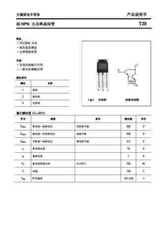
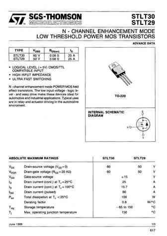
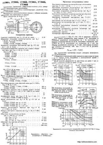
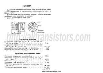
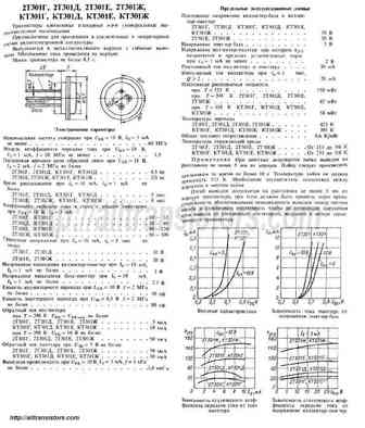
T30 Equivalente. Reemplazo. Hoja de especificaciones. Principales características
Número de Parte: T30
Material: Si
Polaridad de transistor: NPN
ESPECIFICACIONES MÁXIMAS
Disipación total del dispositivo (Pc): 100 W
Tensión colector-base (Vcb): 500 V
Tensión colector-emisor (Vce): 300 V
Tensión emisor-base (Veb): 5 V
Corriente del colector DC máxima (Ic): 10 A
CARACTERÍSTICAS ELÉCTRICAS
Ganancia de corriente contínua (hfe): 1000
Paquete / Cubierta: TO3PN
Búsqueda de reemplazo de T30
T30 datasheet
dmt3009lfvw-7.pdf

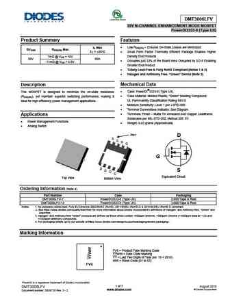
DMT3009LFVW 30V N-CHANNEL ENHANCEMENT MODE MOSFET PowerDI3333-8 (SWP) (Type UX) Product Summary Features and Benefits Low RDS(ON) Ensures On State Losses Are Minimized ID Max BVDSS RDS(ON) Max Small Form Factor Thermally Efficient Package Enables Higher TC = +25 C Density End Products 11m @ VGS = 10V 50A Occupies Just 33% of The Board Area Occupied by
dmt3006lps-13.pdf
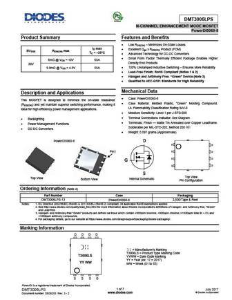
DMT3006LPS Green N-CHANNEL ENHANCEMENT MODE MOSFET PowerDI5060-8 Product Summary Features and Benefits Low RDS(ON) Minimizes On-State Losses ID max Excellent Qgd x RDS(ON) Product (FOM) BVDSS RDS(ON) max TC = +25 C Advanced Technology for DC-DC Converters Small Form Factor Thermally Efficient Package Enables Higher 6m @ VGS = 10V 65A Density En
dmt3006lfv-7.pdf
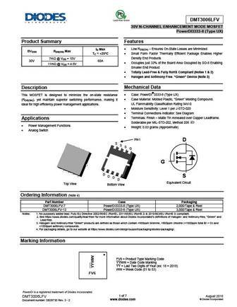
DMT3006LFV 30V N-CHANNEL ENHANCEMENT MODE MOSFET PowerDI3333-8 (Type UX) Product Summary Features Low RDS(ON) Ensures On-State Losses are Minimized ID Max BVDSS RDS(ON) Max TC = +25 Small Form Factor Thermally Efficient Package Enables Higher C Density End Products 7m @ VGS = 10V 30V 60A Occupies just 33% of the Board Area Occupied by SO-8 Enabling
mmft3055v .pdf

MOTOROLA Order this document SEMICONDUCTOR TECHNICAL DATA by MMFT3055V/D Designer's Data Sheet MMFT3055V TMOS V SOT-223 for Surface Mount N Channel Enhancement Mode Silicon Gate TMOS POWER FET TM TMOS V is a new technology designed to achieve an on resis- 1.7 AMPERES tance area product about one half that of standard MOSFETs. This 60 VOLTS new technology more than d
mmft3055el.pdf
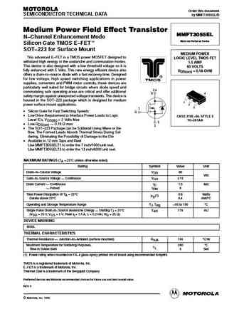
MOTOROLA Order this document SEMICONDUCTOR TECHNICAL DATA by MMFT3055EL/D Medium Power Field Effect Transistor MMFT3055EL N Channel Enhancement Mode Motorola Preferred Device Silicon Gate TMOS E FETt SOT 223 for Surface Mount MEDIUM POWER This advanced E FET is a TMOS power MOSFET designed to LOGIC LEVEL TMOS FET withstand high energy in the avalanche and commutation modes.
mmft3055vl.pdf
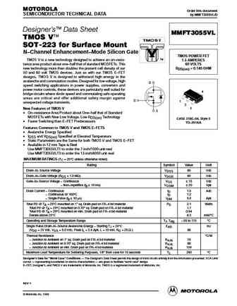
MOTOROLA Order this document SEMICONDUCTOR TECHNICAL DATA by MMFT3055VL/D Designer's Data Sheet MMFT3055VL TMOS V SOT-223 for Surface Mount N Channel Enhancement Mode Silicon Gate TMOS POWER FET TM TMOS V is a new technology designed to achieve an on resis- 1.5 AMPERES tance area product about one half that of standard MOSFETs. This 60 VOLTS new technology more than
mmft3055e.pdf
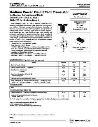
MOTOROLA Order this document SEMICONDUCTOR TECHNICAL DATA by MMFT3055E/D Medium Power Field Effect Transistor MMFT3055E N Channel Enhancement Mode Motorola Preferred Device Silicon Gate TMOS E FETt SOT 223 for Surface Mount MEDIUM POWER This advanced E FET is a TMOS Medium Power MOSFET TMOS FET designed to withstand high energy in the avalanche and commuta- 1.7 AMP tion m
mmft3055v.pdf
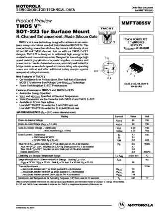
MOTOROLA Order this document SEMICONDUCTOR TECHNICAL DATA by MMFT3055V/D Product Preview MMFT3055V TMOS V SOT-223 for Surface Mount N Channel Enhancement Mode Silicon Gate TMOS POWER FET TM TMOS V is a new technology designed to achieve an on resis- 1.7 AMPERES tance area product about one half that of standard MOSFETs. This 60 VOLTS new technology more than doubles th
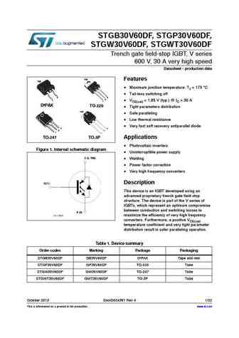
stgb30v60df stgp30v60df stgw30v60df stgwt30v60df.pdf

STGB30V60DF, STGP30V60DF, STGW30V60DF, STGWT30V60DF Trench gate field-stop IGBT, V series 600 V, 30 A very high speed Datasheet - production data TAB Features TAB Maximum junction temperature TJ = 175 C Tail-less switching off 3 3 2 1 VCE(sat) = 1.85 V (typ.) @ IC = 30 A 1 D PAK TO-220 Tight parameters distribution TAB Safe paralleling Low therma
stgwt30h65fb.pdf
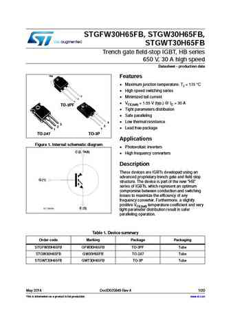
STGFW30H65FB, STGW30H65FB, STGWT30H65FB Trench gate field-stop IGBT, HB series 650 V, 30 A high speed Datasheet - production data TAB Features Maximum junction temperature TJ = 175 C High speed switching series 3 Minimized tail current 2 1 VCE(sat) = 1.55 V (typ.) @ IC = 30 A TO-3PF Tight parameters distribution 1 1 1 Safe paralleling 3 Low t
stgwt30hp65fb.pdf
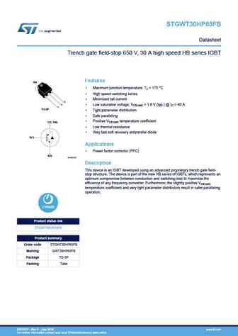
STGWT30HP65FB Datasheet Trench gate field-stop 650 V, 30 A high speed HB series IGBT Features TAB Maximum junction temperature TJ = 175 C High speed switching series Minimized tail current 3 2 Low saturation voltage VCE(sat) = 1.6 V (typ.) @ IC = 40 A 1 TO-3P Tight parameter distribution Safe paralleling Positive VCE(sat) temperature coefficient C
but30v.pdf
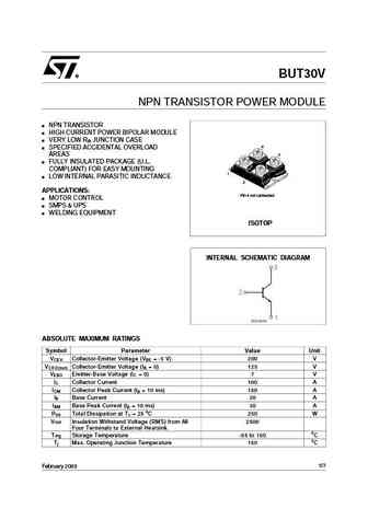
BUT30V NPN TRANSISTOR POWER MODULE NPN TRANSISTOR HIGH CURRENT POWER BIPOLAR MODULE VERY LOW R JUNCTION CASE th SPECIFIED ACCIDENTAL OVERLOAD AREAS FULLY INSULATED PACKAGE (U.L. COMPLIANT) FOR EASY MOUNTING LOW INTERNAL PARASITIC INDUCTANCE APPLICATIONS Pin 4 not connected MOTOR CONTROL SMPS & UPS WELDING EQUIPMENT ISOTOP INTERNAL SCHEMATIC DIAGRAM ABSOLUTE MAX
stgwt30v60f.pdf
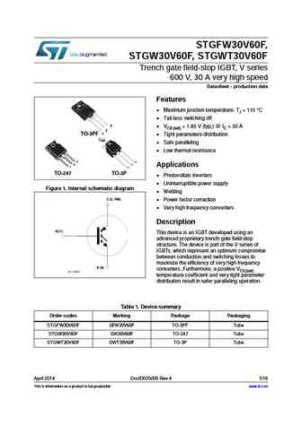
STGFW30V60F, STGW30V60F, STGWT30V60F Trench gate field-stop IGBT, V series 600 V, 30 A very high speed Datasheet - production data Features Maximum junction temperature TJ = 175 C 1 1 1 Tail-less switching off 3 VCE(sat) = 1.85 V (typ.) @ IC = 30 A 2 1 TO-3PF Tight parameters distribution Tab Safe paralleling Low thermal resistance 3 3 2 2 App
stgw30h60dfb stgwa30h60dfb stgwt30h60dfb.pdf
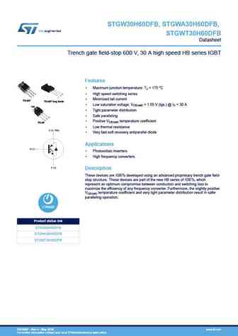
STGW30H60DFB, STGWA30H60DFB, STGWT30H60DFB Datasheet Trench gate field-stop 600 V, 30 A high speed HB series IGBT Features Maximum junction temperature TJ = 175 C 3 3 High speed switching series 2 2 1 1 Minimized tail current TO-247 TO-247 long leads Low saturation voltage VCE(sat) = 1.55 V (typ.) @ IC = 30 A TAB Tight parameter distribution Safe para
stgwt30v60df.pdf
STGB30V60DF, STGP30V60DF, STGW30V60DF, STGWT30V60DF Trench gate field-stop IGBT, V series 600 V, 30 A very high speed Datasheet - production data TAB Features TAB Maximum junction temperature TJ = 175 C Tail-less switching off 3 3 2 1 VCE(sat) = 1.85 V (typ.) @ IC = 30 A 1 D PAK TO-220 Tight parameters distribution TAB Safe paralleling Low therma
stgwt30h60dfb.pdf
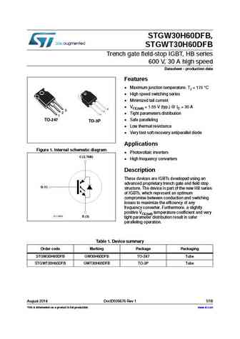
STGW30H60DFB, STGWT30H60DFB Trench gate field-stop IGBT, HB series 600 V, 30 A high speed Datasheet - production data Features Maximum junction temperature TJ = 175 C High speed switching series Minimized tail current VCE(sat) = 1.55 V (typ.) @ IC = 30 A 3 3 2 2 Tight parameters distribution 1 1 TO-247 Safe paralleling TO-3P Low thermal resist
gt30j324.pdf
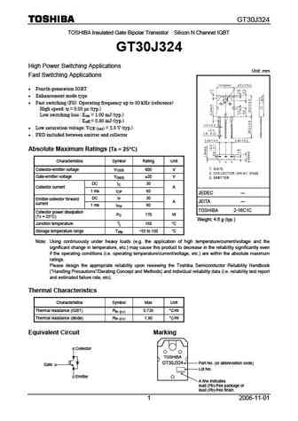
GT30J324 TOSHIBA Insulated Gate Bipolar Transistor Silicon N Channel IGBT GT30J324 High Power Switching Applications Unit mm Fast Switching Applications Fourth-generation IGBT Enhancement mode type Fast switching (FS) Operating frequency up to 50 kHz (reference) High speed tf = 0.05 s (typ.) Low switching loss Eon = 1.00 mJ (typ.) Eoff = 0.80 mJ (ty
gt40t301.pdf
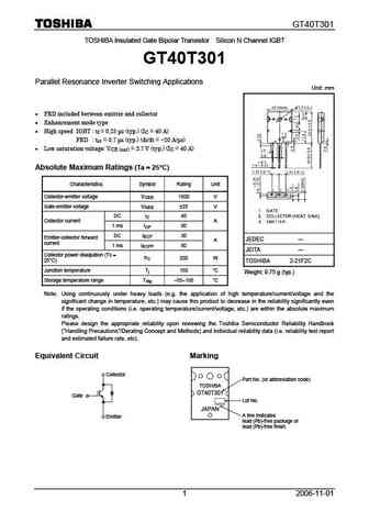
GT40T301 TOSHIBA Insulated Gate Bipolar Transistor Silicon N Channel IGBT GT40T301 Parallel Resonance Inverter Switching Applications Unit mm FRD included between emitter and collector Enhancement mode type High speed IGBT tf = 0.25 s (typ.) (IC = 40 A) FRD trr = 0.7 s (typ.) (di/dt = -20 A/ s) Low saturation voltage VCE (sat) = 3.7 V (typ.) (IC = 40
gt30j322.pdf
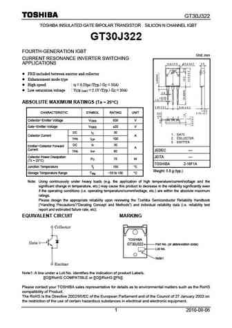
GT30J322 TOSHIBA INSULATED GATE BIPOLAR TRANSISTOR SILICON N CHANNEL IGBT GT30J322 FOURTH-GENERATION IGBT Unit mm CURRENT RESONANCE INVERTER SWITCHING APPLICATIONS FRD included between emitter and collector Enhancement mode type High speed tf = 0.25 s (Typ.) (IC = 50A) Low saturation voltage VCE (sat) = 2.1V (Typ.) (IC = 50A) ABSOLUTE MAXIMUM RATINGS (Ta = 25
gt30j122.pdf
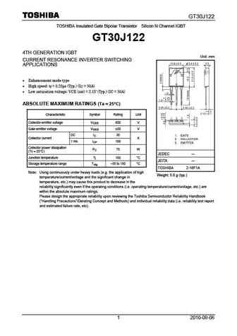
GT30J122 TOSHIBA Insulated Gate Bipolar Transistor Silicon N Channel IGBT GT30J122 4TH GENERATION IGBT Unit mm CURRENT RESONANCE INVERTER SWITCHING APPLICATIONS Enhancement mode type High speed tf = 0.25 s (Typ.) (IC = 50A) Low saturation voltage VCE (sat) = 2.1V (Typ.) (IC = 50A) ABSOLUTE MAXIMUM RATINGS (Ta = 25 C) Characteristic Symbol Rating Unit Coll
gt30j301.pdf
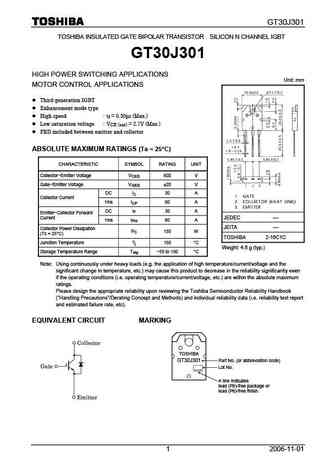
GT30J301 TOSHIBA INSULATED GATE BIPOLAR TRANSISTOR SILICON N CHANNEL IGBT GT30J301 HIGH POWER SWITCHING APPLICATIONS Unit mm MOTOR CONTROL APPLICATIONS Third-generation IGBT Enhancement mode type High speed tf = 0.30 s (Max.) Low saturation voltage VCE (sat) = 2.7V (Max.) FRD included between emitter and collector ABSOLUTE MAXIMUM RATINGS (Ta = 25 C) CHA
gt30j121.pdf
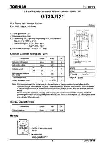
GT30J121 TOSHIBA Insulated Gate Bipolar Transistor Silicon N Channel IGBT GT30J121 High Power Switching Applications Unit mm Fast Switching Applications Fourth-generation IGBT Enhancement mode type Fast switching (FS) Operating frequency up to 50 kHz (reference) High speed tf = 0.05 s (typ.) Low switching loss Eon = 1.00 mJ (typ.) Eoff = 0.80 mJ (typ
gt30j122a.pdf
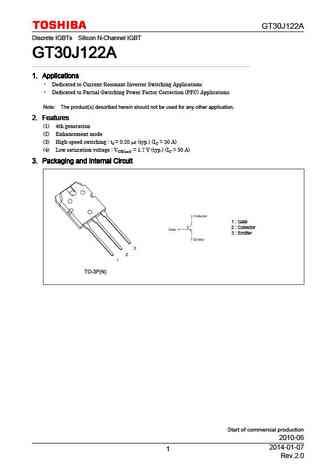
GT30J122A Discrete IGBTs Silicon N-Channel IGBT GT30J122A GT30J122A GT30J122A GT30J122A 1. Applications 1. Applications 1. Applications 1. Applications Dedicated to Current-Resonant Inverter Switching Applications Dedicated to Partial-Switching Power Factor Correction (PFC) Applications Note The product(s) described herein should not be used for any other application. 2. F
gt30j126.pdf
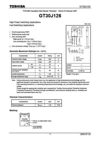
GT30J126 TOSHIBA Insulated Gate Bipolar Transistor Silicon N Channel IGBT GT30J126 High Power Switching Applications Unit mm Fast Switching Applications Fourth-generation IGBT Enhancement mode type Fast switching (FS) High speed tf = 0.05 s (typ.) Low switching loss Eon = 1.00 mJ (typ.) Eoff = 0.80 mJ (typ.) Low saturation voltage VCE (sat) =
rej03g0405 hat3015t.pdf

To our customers, Old Company Name in Catalogs and Other Documents On April 1st, 2010, NEC Electronics Corporation merged with Renesas Technology Corporation, and Renesas Electronics Corporation took over all the business of both companies. Therefore, although the old company name remains in this document, it is a valid Renesas Electronics document. We appreciate your understanding.
rej03g1199 hat3010rds.pdf

To our customers, Old Company Name in Catalogs and Other Documents On April 1st, 2010, NEC Electronics Corporation merged with Renesas Technology Corporation, and Renesas Electronics Corporation took over all the business of both companies. Therefore, although the old company name remains in this document, it is a valid Renesas Electronics document. We appreciate your understanding.
hat3038r.pdf
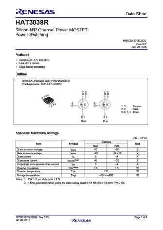
Data Sheet HAT3038R Silicon N/P Channel Power MOSFET Power Switching R07DS1375EJ0301 Rev.3.01 Jan 20, 2017 Features Capable of 4.5 V gate drive Low drive current High density mounting Outline RENESAS Package code PRSP0008DD-D (Package name SOP-8) 7 8 5 6 D D D D 5 6 7 8 2 4 4 3 2 G G 1 1, 3 Source 2, 4 Gate 5, 6, 7, 8 Drain S 1 S 3 N
rej03g1597 hat3029rds.pdf

To our customers, Old Company Name in Catalogs and Other Documents On April 1st, 2010, NEC Electronics Corporation merged with Renesas Technology Corporation, and Renesas Electronics Corporation took over all the business of both companies. Therefore, although the old company name remains in this document, it is a valid Renesas Electronics document. We appreciate your understanding.
rej03g0415 hat3021r.pdf

To our customers, Old Company Name in Catalogs and Other Documents On April 1st, 2010, NEC Electronics Corporation merged with Renesas Technology Corporation, and Renesas Electronics Corporation took over all the business of both companies. Therefore, although the old company name remains in this document, it is a valid Renesas Electronics document. We appreciate your understanding.
rej03g1196 hat3004rds.pdf

To our customers, Old Company Name in Catalogs and Other Documents On April 1st, 2010, NEC Electronics Corporation merged with Renesas Technology Corporation, and Renesas Electronics Corporation took over all the business of both companies. Therefore, although the old company name remains in this document, it is a valid Renesas Electronics document. We appreciate your understanding.
rej03g1198 hat3008rrjds.pdf

To our customers, Old Company Name in Catalogs and Other Documents On April 1st, 2010, NEC Electronics Corporation merged with Renesas Technology Corporation, and Renesas Electronics Corporation took over all the business of both companies. Therefore, although the old company name remains in this document, it is a valid Renesas Electronics document. We appreciate your understanding.
hat3008rj.pdf

To our customers, Old Company Name in Catalogs and Other Documents On April 1st, 2010, NEC Electronics Corporation merged with Renesas Technology Corporation, and Renesas Electronics Corporation took over all the business of both companies. Therefore, although the old company name remains in this document, it is a valid Renesas Electronics document. We appreciate your understanding.
rej03g1368 hat3015rds.pdf
To our customers, Old Company Name in Catalogs and Other Documents On April 1st, 2010, NEC Electronics Corporation merged with Renesas Technology Corporation, and Renesas Electronics Corporation took over all the business of both companies. Therefore, although the old company name remains in this document, it is a valid Renesas Electronics document. We appreciate your understanding.
rej03g1197 hat3006rds.pdf

To our customers, Old Company Name in Catalogs and Other Documents On April 1st, 2010, NEC Electronics Corporation merged with Renesas Technology Corporation, and Renesas Electronics Corporation took over all the business of both companies. Therefore, although the old company name remains in this document, it is a valid Renesas Electronics document. We appreciate your understanding.
hat3037r.pdf
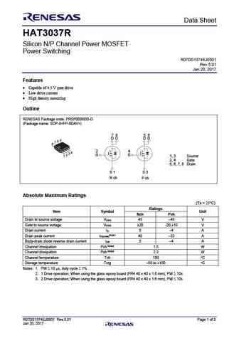
Data Sheet HAT3037R Silicon N/P Channel Power MOSFET Power Switching R07DS1374EJ0501 Rev.5.01 Jan 20, 2017 Features Capable of 4.5 V gate drive Low drive current High density mounting Outline RENESAS Package code PRSP0008DD-D (Package name SOP-8) 7 8 5 6 D D D D 5 6 7 8 2 4 4 3 2 G G 1 1, 3 Source 2, 4 Gate 5, 6, 7, 8 Drain S 1 S 3 N
hat3036r.pdf
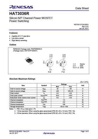
Data Sheet HAT3036R Silicon N/P Channel Power MOSFET Power Switching R07DS1373EJ0501 Rev.5.01 Jan 20, 2017 Features Capable of 4.5 V gate drive Low drive current High density mounting Outline RENESAS Package code PRSP0008DD-D (Package name SOP-8) 7 8 5 6 D D D D 5 6 7 8 2 4 4 G G 3 2 1 1, 3 Source 2, 4 Gate 5, 6, 7, 8 Drain S 1 S 3
hat3018rj.pdf

To our customers, Old Company Name in Catalogs and Other Documents On April 1st, 2010, NEC Electronics Corporation merged with Renesas Technology Corporation, and Renesas Electronics Corporation took over all the business of both companies. Therefore, although the old company name remains in this document, it is a valid Renesas Electronics document. We appreciate your understanding.
rej03g0127 hat3018r.pdf

To our customers, Old Company Name in Catalogs and Other Documents On April 1st, 2010, NEC Electronics Corporation merged with Renesas Technology Corporation, and Renesas Electronics Corporation took over all the business of both companies. Therefore, although the old company name remains in this document, it is a valid Renesas Electronics document. We appreciate your understanding.
hat3019r.pdf
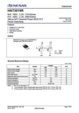
Preliminary Datasheet HAT3019R Nch 100V, 3.5A, 115m max. Pch -100V, -2.3A, 300m max R07DS1324EJ0700 Silicon N/P Channel Power MOS FET Rev.7.00 Feb 18, 2016 Power Switching Features Capable of 4.5 V gate drive Low drive current High density mounting Pb-free Outline RENESAS Package code PRSP0008DD-D (Package name SOP-8) 7 8 5 6 D D D
ndt3055.pdf
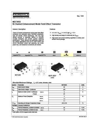
May 1998 NDT3055 N-Channel Enhancement Mode Field Effect Transistor General Description Features These N-Channel enhancement mode power field effect 4 A, 60 V. RDS(ON) = 0.100 @ VGS = 10 V. transistors are produced using Fairchild's proprietary, High density cell design for extremely low RDS(ON). high cell density, DMOS technology. This very high density process is especially t
ndt3055l.pdf
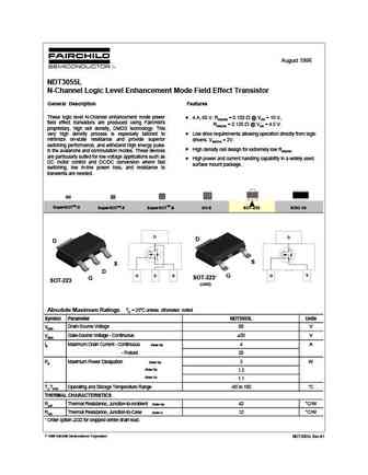
August 1998 NDT3055L N-Channel Logic Level Enhancement Mode Field Effect Transistor General Description Features These logic level N-Channel enhancement mode power 4 A, 60 V. RDS(ON) = 0.100 @ VGS = 10 V, field effect transistors are produced using Fairchild's RDS(ON) = 0.120 @ VGS = 4.5 V. proprietary, high cell density, DMOS technology. This very high density process is
fzt3019.pdf
April 2006 FZT3019 tm NPN General Purpose Amplifier 4 Features This device is designed for general purpose medium power amplifiers and switches requiring collector currents to 500 mA and collector voltages up to 80 V. 3 Sourced from process 12. 2 1 SOT-223 1. Base 2. Collector 3. Emitter Absolute Maximum Ratings * Ta = 25 C unless otherwise noted Symbol Parameter Value U
fdms8050et30.pdf
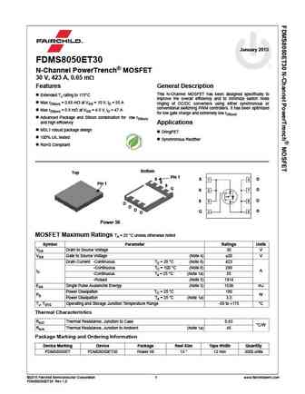
January 2015 FDMS8050ET30 N-Channel PowerTrench MOSFET 30 V, 423 A, 0.65 m Features General Description This N-Channel MOSFET has been designed specifically to Extended TJ rating to 175 C improve the overall efficiency and to minimize switch node Max rDS(on) = 0.65 m at VGS = 10 V, ID = 55 A ringing of DC/DC converters using either synchronous or conventional switching PWM
fdmc8010et30.pdf
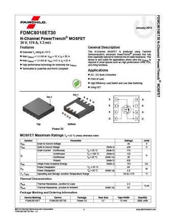
January 2015 FDMC8010ET30 N-Channel PowerTrench MOSFET 30 V, 174 A, 1.3 m Features General Description This N-Channel MOSFET is produced using Fairchild Extended TJ rating to 175 C Semiconductor s advanced PowerTrench process that has Max rDS(on) = 1.3 m at VGS = 10 V, ID = 30 A been especially tailored to minimize the on-state resistance. This device is well suited for
sct3060al.pdf
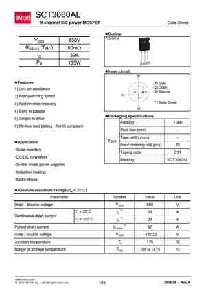
SCT3060AL N-channel SiC power MOSFET Data Sheet lOutline TO-247N VDSS 650V RDS(on) (Typ.) 60mW ID 39A (3) PD 165W (2) (1) lInner circuit lFeatures (1) Gate (2) Drain 1) Low on-resistance (3) Source 2) Fast switching speed *1 Body Diode 3) Fast reverse recovery 4) Easy to parallel lPackaging specifications 5) Simple to drive Packing Tube 6) Pb-free lead plating
rgt30ns65d.pdf
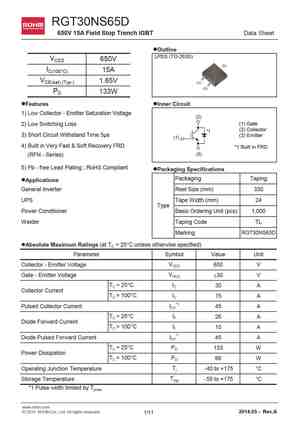
RGT30NS65D 650V 15A Field Stop Trench IGBT Data Sheet lOutline LPDS (TO-263S) VCES 650V (2) IC(100 C) 15A VCE(sat) (Typ.) 1.65V (1) (3) PD 133W lFeatures lInner Circuit 1) Low Collector - Emitter Saturation Voltage (2) (1) Gate 2) Low Switching Loss (2) Collector *1 3) Short Circuit Withstand Time 5 s (3) Emitter (1) 4) Built in Very Fast & Soft Recovery FR
sct3080kl.pdf
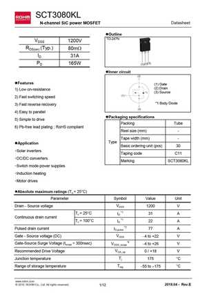
SCT3080KL N-channel SiC power MOSFET Datasheet Outline TO-247N VDSS 1200V RDS(on) (Typ.) 80m ID 31A (3) PD 165W (2) (1) Inner circuit (2) Features (1) Gate (2) Drain 1) Low on-resistance (3) Source *1 (1) 2) Fast switching speed *1 Body Diode 3) Fast reverse recovery (3) 4) Easy to parallel Packaging specifications 5) Simple to drive Packing Tube
sct3080klhr.pdf

SCT3080KLHR Automotive Grade N-channel SiC power MOSFET Datasheet lOutline TO-247N VDSS 1200V RDS(on) (Typ.) 80m 31A ID*1 PD (3) 165W (2) (1) lInner circuit lFeatures (1) Gate 1) Qualified to AEC-Q101 (2) Drain (3) Source 2) Low on-resistance *Body Diode 3) Fast switching speed 4) Fast reverse recovery Please note Driver Source and Power Source are 5) Easy to p
sct3060ar.pdf

SCT3060AR N-channel SiC power MOSFET Datasheet lOutline TO-247-4L VDSS 650V RDS(on) (Typ.) 60m 39A ID*1 PD 165W (1) (2)(3)(4) lInner circuit lFeatures 1) Low on-resistance 2) Fast switching speed 3) Fast reverse recovery 4) Easy to parallel Please note Driver Source and Power Source are 5) Simple to drive not exchangeable. Their exchange might lead to malfunction. 6) P
vs-gt300fd060n.pdf

VS-GT300FD060N www.vishay.com Vishay Semiconductors DIAP Low Profile 3-Levels Half Bridge Inverter Stage, 300 A FEATURES Trench plus Field Stop IGBT technology FRED Pt antiparallel and clamping diodes Short circuit capability Low stray internal inductances Low switching loss UL approved file E78996 Material categorization for definitions of compliance
vs-gt300yh120n.pdf
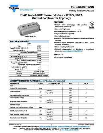
VS-GT300YH120N www.vishay.com Vishay Semiconductors DIAP Trench IGBT Power Module - 1200 V, 300 A Current Fed Inverter Topology FEATURES Trench IGBT technology with positive temperature coefficient Low switching losses Maximum junction temperature 150 C 10 s short circuit capability Low inductance case Double INT-A-PAK HEXFRED antiparallel and series
j308 sst308 j309 sst309 j310 sst310 u309 u310.pdf
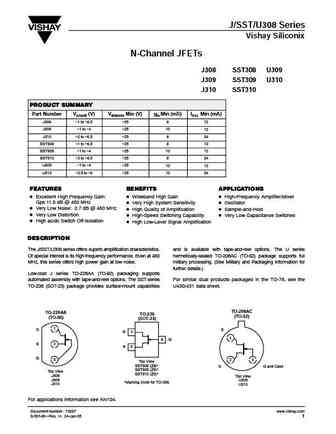
J/SST/U308 Series Vishay Siliconix N-Channel JFETs J308 SST308 U309 J309 SST309 U310 J310 SST310 PRODUCT SUMMARY Part Number VGS(off) (V) V(BR)GSS Min (V) gfs Min (mS) IDSS Min (mA) J308 -1 to -6.5 -25 8 12 J309 -1 to -4 -25 10 12 J310 -2 to -6.5 -25 8 24 SST308 -1 to -6.5 -25 8 12 SST309 -1 to -4 -25 10 12 SST310 -2 to -6.5 -25 8 24 U309 -1 to -4 -25 10 12 U310 -2.5 to -6 -25 10
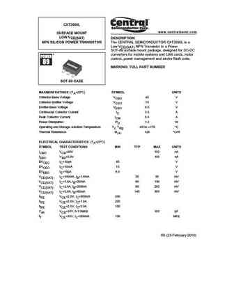
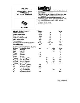
cxt3090l.pdf
CXT3090L www.centralsemi.com SURFACE MOUNT LOW VCE(SAT) DESCRIPTION NPN SILICON POWER TRANSISTOR The CENTRAL SEMICONDUCTOR CXT3090L is a Low VCE(SAT) NPN Transistor in a Power SOT-89 surface mount package, designed for DC-DC converters for mobile systems and LAN cards, motor control, power management and strobe flash units. MARKING FULL PART NUMBER SOT-89 CASE MAXIMUM RATINGS
czt2955 czt3055.pdf
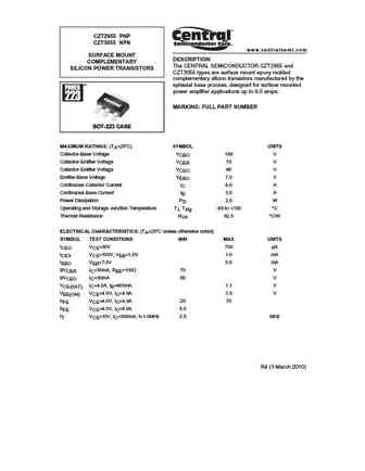
CZT2955 PNP CZT3055 NPN www.centralsemi.com SURFACE MOUNT DESCRIPTION COMPLEMENTARY The CENTRAL SEMICONDUCTOR CZT2955 and SILICON POWER TRANSISTORS CZT3055 types are surface mount epoxy molded complementary silicon transistors manufactured by the epitaxial base process, designed for surface mounted power amplifier applications up to 6.0 amps. MARKING FULL PART NUMBER SOT-223
czt3090le.pdf
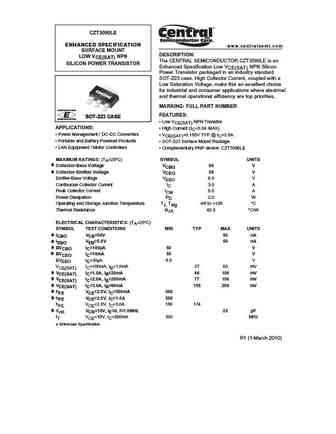
CZT3090LE ENHANCED SPECIFICATION www.centralsemi.com SURFACE MOUNT DESCRIPTION LOW VCE(SAT) NPN The CENTRAL SEMICONDUCTOR CZT3090LE is an SILICON POWER TRANSISTOR Enhanced Specification Low VCE(SAT) NPN Silicon Power Transistor packaged in an industry standard SOT-223 case. High Collector Current, coupled with a Low Saturation Voltage, make this an excellent choice for industrial
czt3019.pdf
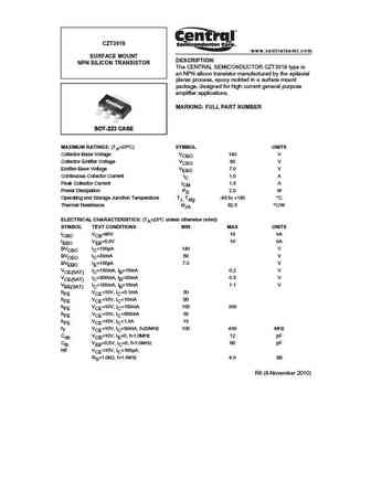
CZT3019 www.centralsemi.com SURFACE MOUNT DESCRIPTION NPN SILICON TRANSISTOR The CENTRAL SEMICONDUCTOR CZT3019 type is an NPN silicon transistor manufactured by the epitaxial planar process, epoxy molded in a surface mount package, designed for high current general purpose amplifier applications. MARKING FULL PART NUMBER SOT-223 CASE SOT-223 CASE MAXIMUM RATINGS (TA=25 C) S
czt3090l.pdf
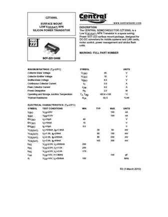
CZT3090L www.centralsemi.com SURFACE MOUNT LOW VCE(SAT) NPN DESCRIPTION SILICON POWER TRANSISTOR The CENTRAL SEMICONDUCTOR CZT3090L is a Low VCE(SAT) NPN Transistor in a space saving Power SOT-223 surface mount package, designed for DC-DC converters for mobile systems and LAN cards, motor control, power management and strobe flash units. MARKING FULL PART NUMBER SOT-223 CASE
cmxt3090l.pdf
CMXT3090L www.centralsemi.com SURFACE MOUNT SILICON LOW VCE(SAT) DESCRIPTION NPN POWER TRANSISTOR The CENTRAL SEMICONDUCTOR CMXT3090L is a low VCE(SAT) NPN transistor in a six lead Power SOT-26 surface mount package designed for LAN cards, motor control, power management, strobe flash units and DC-DC converters for mobile systems. MARKING CODE X309L SOT-26 CASE MAXIMUM RATINGS
dmt3020lsd.pdf
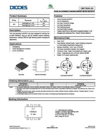
DMT3020LSD DUAL N-CHANNEL ENHANCEMENT MODE MOSFET Product Summary Features ID Dual N-Channel MOSFET BVDSS RDS(ON) Max TA = +25 C Low On-Resistance Low Gate Threshold Voltage 20m @ VGS = 10V 16A 30V Low Input Capacitance 32m @ VGS = 4.5V 13A Fast Switching Speed Low Input/Output Leakage Description Totally Lead-Free & Fully RoHS Comp
dmt3002lps.pdf
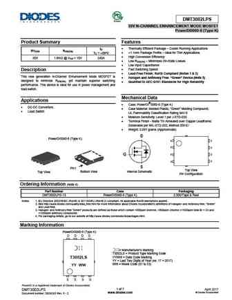
DMT3002LPS Green 30V N-CHANNEL ENHANCEMENT MODE MOSFET PowerDI5060-8 (Type K) Product Summary Features Thermally Efficient Package Cooler Running Applications ID BVDSS RDS(ON) TC = +25 C
dmt3020lfdb.pdf
DMT3020LFDB DUAL N-CHANNEL ENHANCEMENT MODE MOSFET Product Summary Features and Benefits 0.6mm Profile Ideal for Low Profile Applications ID Max V(BR)DSS RDS(ON) Max TA = +25 C Low Gate Threshold Voltage Low On-Resistance 7.7A 20m @ VGS = 10V Totally Lead-Free & Fully RoHS Compliant (Notes 1 & 2) 30V 32m @ VGS = 4.5V 6.1A Halogen and An
dmt3009lfvw.pdf
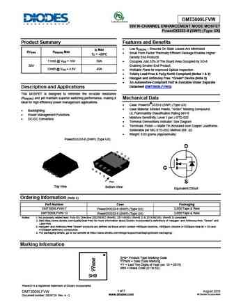
DMT3009LFVW 30V N-CHANNEL ENHANCEMENT MODE MOSFET PowerDI3333-8 (SWP) (Type UX) Product Summary Features and Benefits Low RDS(ON) Ensures On State Losses Are Minimized ID Max BVDSS RDS(ON) Max Small Form Factor Thermally Efficient Package Enables Higher TC = +25 C Density End Products 11m @ VGS = 10V 50A Occupies Just 33% of The Board Area Occupied by
dmt3009ldt.pdf
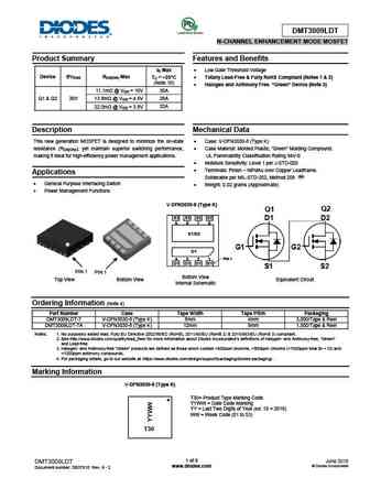
DMT3009LDT N-CHANNEL ENHANCEMENT MODE MOSFET Product Summary Features and Benefits ID Max Low Gate Threshold Voltage Device BVDSS RDS(ON) Max TC = +25 Totally Lead-Free & Fully RoHS Compliant (Notes 1 & 2) C (Note 10) Halogen and Antimony Free. Green Device (Note 3) 11.1m @ VGS = 10V 30A Q1 & Q2 30V 13.8m @ VGS = 4.5V 28A 22.0m @ VGS = 3.8V 22A
dmt3020lfdf.pdf
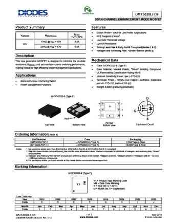
DMT3020LFDF 30V N-CHANNEL ENHANCEMENT MODE MOSFET Product Summary Features 0.6mm Profile Ideal for Low Profile Applications ID max V(BR)DSS RDS(ON) max PCB Footprint of 4mm2 TA = +25 C Low Gate Threshold Voltage 17m @ VGS = 10V 8.4A Low On-Resistance 30V 28m @ VGS = 4.5V 6.8A Totally Lead-Free & Fully RoHS Compliant (Notes 1 & 2)
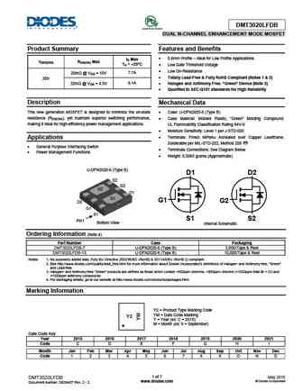
dmt3006lps.pdf

DMT3006LPS Green N-CHANNEL ENHANCEMENT MODE MOSFET PowerDI5060-8 Product Summary Features and Benefits Low RDS(ON) Minimizes On-State Losses ID max Excellent Qgd x RDS(ON) Product (FOM) BVDSS RDS(ON) max TC = +25 C Advanced Technology for DC-DC Converters Small Form Factor Thermally Efficient Package Enables Higher 6m @ VGS = 10V 65A Density En
dmt3006lfv.pdf
DMT3006LFV 30V N-CHANNEL ENHANCEMENT MODE MOSFET PowerDI3333-8 (Type UX) Product Summary Features Low RDS(ON) Ensures On-State Losses are Minimized ID Max BVDSS RDS(ON) Max TC = +25 Small Form Factor Thermally Efficient Package Enables Higher C Density End Products 7m @ VGS = 10V 30V 60A Occupies just 33% of the Board Area Occupied by SO-8 Enabling
ixgt30n60c3d1.pdf
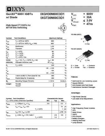
GenX3TM 600V IGBTs VCES = 600V IXGH30N60C3D1 w/ Diode IC110 = 30A IXGT30N60C3D1 VCE(sat) 3.0V tfi(typ) = 47ns High-Speed PT IGBTs for 40-100 kHz Switching TO-268 (IXGT) Symbol Test Conditions Maximum Ratings G VCES TC = 25 C to 150 C 600 V E VCGR TJ = 25 C to 150 C, RGE = 1M 600 V C (Tab) VGES Continuous 20 V VGEM Transient 30 V TO-247 (IXG
ixth30n50l2-ixtq30n50l2-ixtt30n50l2.pdf
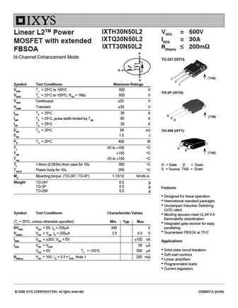
IXTH30N50L2 VDSS = 500V Linear L2TM Power IXTQ30N50L2 ID25 = 30A MOSFET with extended IXTT30N50L2 RDS(on) 200m FBSOA D D D D O D O N-Channel Enhancement Mode TO-247 (IXTH) RGi w w G O O (TAB) S Symbol Test Conditions Maximum Ratings VDSS TJ = 25 C to 150 C 500 V TO-3P (IXTQ) VDGR TJ = 25 C to 150 C, RGS = 1M 500 V VGSS Continu
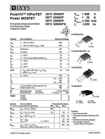
ixfh30n50p ixft30n50p ixfv30n50p.pdf
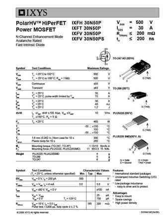
VDSS = 500 V IXFH 30N50P PolarHVTM HiPerFET ID25 = 30 A IXFT 30N50P Power MOSFET RDS(on) 200 m IXFV 30N50P N-Channel Enhancement Mode trr 200 ns IXFV 30N50PS Avalanche Rated Fast Intrinsic Diode TO-247 AD (IXFH) Symbol Test Conditions Maximum Ratings VDSS TJ = 25 C to 150 C 500 V D (TAB) VDGR TJ = 25 C to
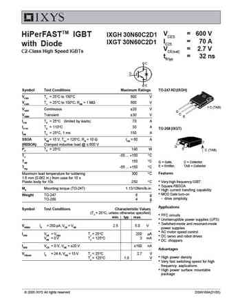
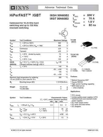
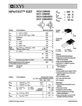
ixgh30n60c2 ixgt30n60c2.pdf

VCES = 600 V IXGH 30N60C2 HiPerFASTTM IGBT IC25 = 70 A IXGT 30N60C2 VCE(sat) = 2.7 V C2-Class High Speed IGBTs tfi typ = 32 ns TO-268 (IXGT) Symbol Test Conditions Maximum Ratings VCES TJ = 25 C to 150 C 600 V VCGR TJ = 25 C to 150 C; RGE = 1 M 600 V G E C (TAB) VGES Continuous 20 V VGEM Transient 30 V IC25 TC = 25 C (limited by leads) 70 A TO-247 (IXGH) IC110 TC =
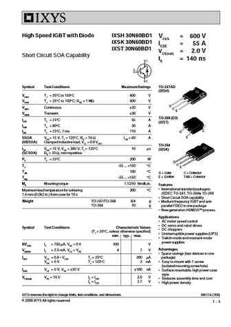
ixst30n60cd1.pdf
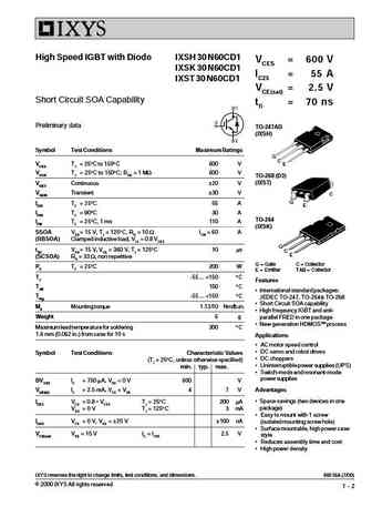
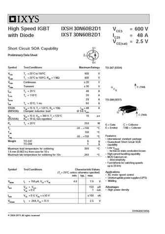
High Speed IGBT with Diode IXSH 30 N60CD1 VCES = 600 V IXSK 30 N60CD1 IC25 = 55 A IXST 30 N60CD1 VCE(sat) = 2.5 V Short Circuit SOA Capability tfi = 70 ns Preliminary data TO-247AD (IXSH) Symbol Test Conditions Maximum Ratings G C VCES TJ = 25 C to 150 C 600 V E VCGR TJ = 25 C to 150 C; RGE = 1 MW 600 V TO-268 (D3) (IXST) VGES Continuous 20 V VGEM Transient 30 V C G
ixgt30n60c2.pdf
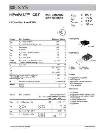
VCES = 600 V IXGH 30N60C2 HiPerFASTTM IGBT IC25 = 70 A IXGT 30N60C2 VCE(sat) = 2.7 V C2-Class High Speed IGBTs tfi typ = 32 ns TO-268 (IXGT) Symbol Test Conditions Maximum Ratings VCES TJ = 25 C to 150 C 600 V VCGR TJ = 25 C to 150 C; RGE = 1 M 600 V G E C (TAB) VGES Continuous 20 V VGEM Transient 30 V IC25 TC = 25 C (limited by leads) 70 A TO-247 (IXGH) IC110 TC =
ixfh30n50 ixfh32n50 ixft30n50 ixft32n50.pdf
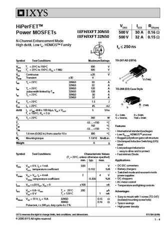
VDSS ID25 RDS(on) HiPerFETTM IXFH/IXFT 30N50 500 V 30 A 0.16 W Power MOSFETs IXFH/IXFT 32N50 500 V 32 A 0.15 W N-Channel Enhancement Mode High dv/dt, Low trr, HDMOSTM Family trr 250 ns TO-247 AD (IXFH) Symbol Test Conditions Maximum Ratings VDSS TJ = 25 C to 150 C 500 V VDGR TJ = 25 C to 150 C; RGS = 1 MW 500 V VGS Continuous 20 V VGSM Transient 30 V D (TAB) ID25 TC
ixgh30n60c2d1 ixgt30n60c2d1.pdf

VCES = 600 V HiPerFASTTM IGBT IXGH 30N60C2D1 IC25 = 70 A IXGT 30N60C2D1 with Diode VCE(sat) = 2.7 V C2-Class High Speed IGBTs tfi typ = 32 ns Symbol Test Conditions Maximum Ratings TO-247 AD (IXGH) VCES TJ = 25 C to 150 C 600 V VCGR TJ = 25 C to 150 C; RGE = 1 M 600 V C (TAB) VGES Continuous 20 V G C VGEM Transient 30 V E IC25 TC = 25 C (limited by leads) 70 A IC11
ixst30n60b.pdf

VCES ICES tfi High Speed IGBT IXSH/IXST 30N60B 600 V 2.0 V 140 ns IXSH/IXST 30N60C 600 V 2.5 V 70 ns Short Circuit SOA Capability TO-247 AD (IXSH) Symbol Test Conditions Maximum Ratings VCES TJ = 25 C to 150 C 600 V (TAB) VCGR TJ = 25 C to 150 C; RGE = 1 M 600 V VGES Continuous 20 V VGEM Transient 30 V TO-268 (D3) ( IXST) IC25 TC = 25 C55 A IC90 TC = 90 C30 A G ICM
ixft30n50q.pdf
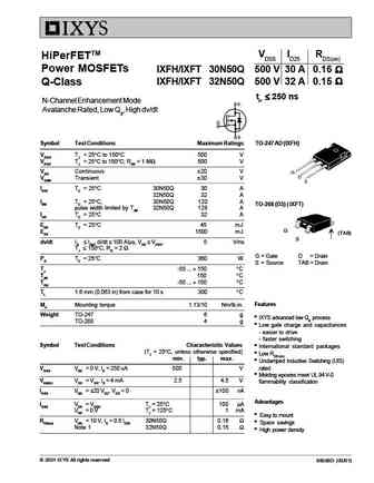
VDSS ID25 RDS(on) HiPerFETTM Power MOSFETs IXFH/IXFT 30N50Q 500 V 30 A 0.16 IXFH/IXFT 32N50Q 500 V 32 A 0.15 Q-Class trr 250 ns N-Channel Enhancement Mode Avalanche Rated, Low Qg, High dv/dt Symbol Test Conditions Maximum Ratings TO-247 AD (IXFH) VDSS TJ = 25 C to 150 C 500 V VDGR TJ = 25 C to 150 C; RGS =
ixgt30n120b3d1.pdf
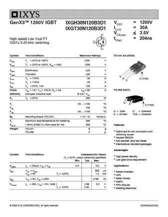
VCES = 1200V GenX3TM 1200V IGBT IXGH30N120B3D1 IC110 = 30A IXGT30N120B3D1 VCE(sat) 3.5V tfi(typ) = 204ns High speed Low Vsat PT IGBTs 3-20 kHz switching Symbol Test Conditions Maximum Ratings TO-247 AD (IXGH) VCES TJ = 25 C to 150 C 1200 V VCGR TJ = 25 C to 150 C, RGE = 1M 1200 V VGES Continuous 20 V VGEM Transient 30 V G IC110 TC = 110 C30
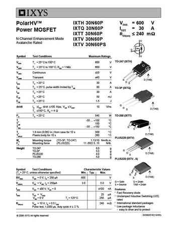
ixth30n50p ixtq30n50p ixtt30n50p ixtv30n50p.pdf
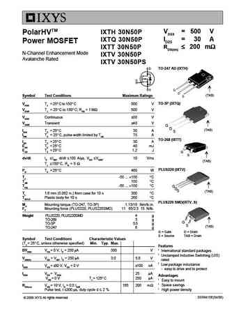
VDSS = 500 V IXTH 30N50P PolarHVTM ID25 = 30 A IXTQ 30N50P Power MOSFET RDS(on) 200 m IXTT 30N50P N-Channel Enhancement Mode IXTV 30N50P Avalanche Rated IXTV 30N50PS TO-247 AD (IXTH) (TAB) Symbol Test Conditions Maximum Ratings TO-3P (IXTQ) VDSS TJ = 25 C to 150 C 500 V VDGR TJ = 25 C to 150 C; RGS = 1 M 500 V VGSS Continuo
ixsh30n60 ixst30n60.pdf

VCES ICES tfi High Speed IGBT IXSH/IXST 30N60B 600 V 2.0 V 140 ns IXSH/IXST 30N60C 600 V 2.5 V 70 ns Short Circuit SOA Capability TO-247 AD (IXSH) Symbol Test Conditions Maximum Ratings VCES TJ = 25 C to 150 C 600 V (TAB) VCGR TJ = 25 C to 150 C; RGE = 1 M 600 V VGES Continuous 20 V VGEM Transient 30 V TO-268 (D3) ( IXST) IC25 TC = 25 C55 A IC90 TC = 90 C30 A G ICM
ixgt30n60c2d1.pdf
VCES = 600 V HiPerFASTTM IGBT IXGH 30N60C2D1 IC25 = 70 A IXGT 30N60C2D1 with Diode VCE(sat) = 2.7 V C2-Class High Speed IGBTs tfi typ = 32 ns Symbol Test Conditions Maximum Ratings TO-247 AD (IXGH) VCES TJ = 25 C to 150 C 600 V VCGR TJ = 25 C to 150 C; RGE = 1 M 600 V C (TAB) VGES Continuous 20 V G C VGEM Transient 30 V E IC25 TC = 25 C (limited by leads) 70 A IC11
ixyt30n450hv.pdf
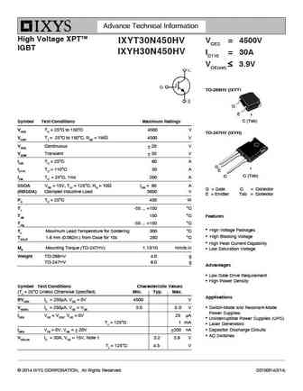
Advance Technical Information High Voltage XPTTM VCES = 4500V IXYT30N450HV IGBT IXYH30N450HV IC110 = 30A VCE(sat) 3.9V TO-268HV (IXYT) G E C (Tab) Symbol Test Conditions Maximum Ratings VCES TC = 25 C to 150 C 4500 V TO-247HV (IXYH) VCGR TJ = 25 C to 150 C, RGE = 1M 4500 V VGES Continuous 20 V VGEM Transient 30 V IC25 TC = 25 C 60 A G I
ixgt30n60b2.pdf

Advance Technical Data VCES = 600 V IXGH 30N60B2 HiPerFASTTM IGBT IC25 = 70 A IXGT 30N60B2 VCE(sat)
ixst30n60bd1.pdf
High Speed IGBT with Diode IXSH 30N60BD1 VCES = 600 V IXSK 30N60BD1 IC25 = 55 A IXST 30N60BD1 VCE(sat) = 2.0 V Short Circuit SOA Capability tfi = 140 ns Symbol Test Conditions Maximum Ratings TO-247AD (IXSH) VCES TJ = 25 C to 150 C 600 V VCGR TJ = 25 C to 150 C; RGE = 1 MW 600 V G VGES Continuous 20 V C E VGEM Transient 30 V TO-268 (D3) IC25 TC = 25 C55 A (IXST) IC9
ixgh30n60b2 ixgt30n60b2.pdf
Advance Technical Data VCES = 600 V IXGH 30N60B2 HiPerFASTTM IGBT IC25 = 70 A IXGT 30N60B2 VCE(sat)
ixfh30n60x ixfq30n60x ixft30n60x.pdf
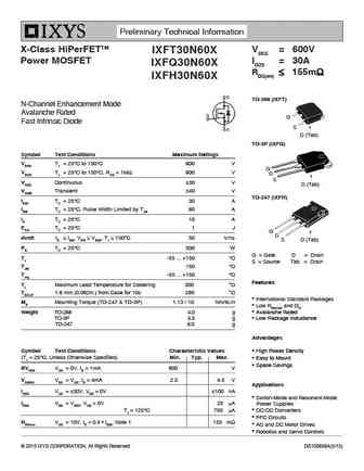
Preliminary Technical Information X-Class HiPerFETTM VDSS = 600V IXFT30N60X Power MOSFET ID25 = 30A IXFQ30N60X RDS(on) 155m IXFH30N60X TO-268 (IXFT) N-Channel Enhancement Mode Avalanche Rated G Fast Intrinsic Diode S D (Tab) TO-3P (IXFQ) Symbol Test Conditions Maximum Ratings VDSS TJ = 25 C to 150 C 600 V G VDGR TJ = 25 C to 150
ixft30n60q.pdf
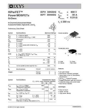
IXFH 30N60Q VDSS = 600 V HiPerFETTM IXFT 30N60Q ID25 = 30 A Power MOSFETs RDS(on) = 0.23 Q-Class trr 250 ns N-Channel Enhancement Mode Avalanche Rated, High dv/dt, Low Qg Preliminary Data Sheet Symbol Test Conditions Maximum Ratings TO-247 AD (IXFH) VDSS TJ = 25 C to 150 C 600 V VDGR TJ = 25 C to 150 C; RGS = 1 M 600 V (TAB
ixgt30n60b2d1.pdf

Advance Technical Data VCES = 600 V HiPerFASTTM IGBT IXGH 30N60B2D1 IC25 = 70 A IXGT 30N60B2D1 VCE(sat)
ixsh30n60b2d1 ixst30n60b2d1.pdf
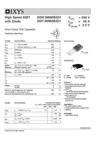
High Speed IGBT IXSH 30N60B2D1 VCES = 600 V IXST 30N60B2D1 with Diode IC25 = 48 A VCE(sat) = 2.5 V Short Circuit SOA Capability Preliminary Data Sheet Symbol Test Conditions Maximum Ratings TO-247 (IXSH) VCES TJ = 25 C to 150 C 600 V VCGR TJ = 25 C to 150 C; RGE = 1 M 600 V VGES Continuous 20 V VGEM Transient 30 V C (TAB) G C E IC25 TC = 25 C48 A IC110 TC = 110 C

ixgt30n60b.pdf
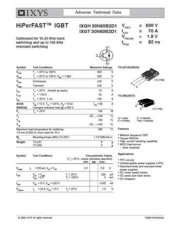
IXGH 32N60B HiPerFASTTM IGBT VCES = 600 V IXGT 32N60B IC25 = 60 A IXGH 32N60BD1 VCE(sat) = 2.3 V IXGT 32N60BD1 tfi(typ) = 85 ns (D1) Symbol Test Conditions Maximum Ratings TO-268 (IXGT) G VCES TJ = 25 C to 150 C 600 V E C VCGR TJ = 25 C to 150 C; RGE = 1 M 600 V (TAB) VGES Continuous 20 V TO-247 AD VGEM Transient 30 V (IXGH) IC25 TC = 25 C60 A IC90 TC = 90 C3
ixdh30n120 ixdt30n120 ixdh30n120d1 ixdt30n120d1.pdf
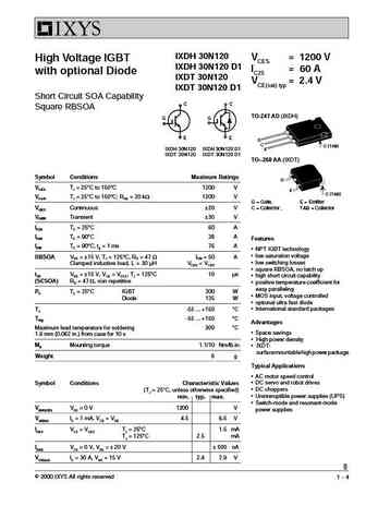
IXDH 30N120 VCES = 1200 V High Voltage IGBT IXDH 30N120 D1 IC25 = 60 A with optional Diode IXDT 30N120 VCE(sat) typ = 2.4 V IXDT 30N120 D1 Short Circuit SOA Capability C C Square RBSOA TO-247 AD (IXDH) G G E E G C C (TAB) IXDH 30N120 IXDH 30N120 D1 E IXDT 30N120 IXDT 30N120 D1 TO--268 AA (IXDT) Symbol Conditions Maximum Ratings G VCES TJ = 25 C to 150 C 1200 V E C (T
ixfh30n60p ixfv30n60p ixft30n60p.pdf
IXFH 30N60P VDSS = 600 V PolarHVTM HiPerFET IXFT 30N60P ID25 = 30 A Power MOSFET IXFV 30N60P RDS(on) 240 m N-Channel Enhancement Mode IXFV 30N60PS trr 200 ns Fast Recovery Diode Avalanche Rated PLUS220 (IXFV) Symbol Test Conditions Maximum Ratings VDSS TJ = 25 C to 150 C 600 V G VDGR TJ = 25 C to 150 C; RGS
ixst30n60c.pdf
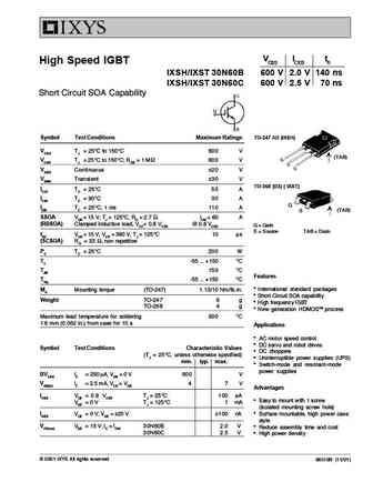
VCES ICES tfi High Speed IGBT IXSH/IXST 30N60B 600 V 2.0 V 140 ns IXSH/IXST 30N60C 600 V 2.5 V 70 ns Short Circuit SOA Capability TO-247 AD (IXSH) Symbol Test Conditions Maximum Ratings VCES TJ = 25 C to 150 C 600 V (TAB) VCGR TJ = 25 C to 150 C; RGE = 1 M 600 V VGES Continuous 20 V VGEM Transient 30 V TO-268 (D3) ( IXST) IC25 TC = 25 C55 A IC90 TC = 90 C30 A G ICM
ixdh30n120au1 ixdt30n120au1.pdf
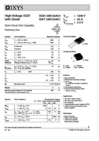
High Voltage IGBT IXDH 30N120AU1 VCES = 1200 V IXDT 30N120AU1 IC25 = 50 A with Diode VCE(sat) typ = 2.5 V Short Circuit SOA Capability Preliminary Data Symbol Test Conditions Maximum Ratings TO-247 AD (IXDH) VCES TJ = 25 C to 150 C 1200 V VCGR TJ = 25 C to 150 C; RGE = 1 M 1200 V C (TAB) G VGES Continuous 20 V C E VGEM Transient 30 V TO-268 AA (IXDT) IC25 TC = 25 C5
ixgh30n60b2d1 ixgt30n60b2d1.pdf
Advance Technical Data VCES = 600 V HiPerFASTTM IGBT IXGH 30N60B2D1 IC25 = 70 A IXGT 30N60B2D1 VCE(sat)
ixst30n60b2d1.pdf
High Speed IGBT IXSH 30N60B2D1 VCES = 600 V IXST 30N60B2D1 with Diode IC25 = 48 A VCE(sat) = 2.5 V Short Circuit SOA Capability Preliminary Data Sheet Symbol Test Conditions Maximum Ratings TO-247 (IXSH) VCES TJ = 25 C to 150 C 600 V VCGR TJ = 25 C to 150 C; RGE = 1 M 600 V VGES Continuous 20 V VGEM Transient 30 V C (TAB) G C E IC25 TC = 25 C48 A IC110 TC = 110 C
ixyt30n65c3h1hv.pdf
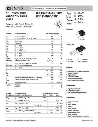
Preliminary Technical Information XPTTM 650V IGBT VCES = 650V IXYT30N65C3H1HV GenX3TM w/ Sonic IC110 = 30A IXYH30N65C3H1 Diode VCE(sat) 2.7V tfi(typ) = 24ns Extreme Light Punch Through IGBT for 20-60kHz Switching TO-268HV Symbol Test Conditions Maximum Ratings G VCES TJ = 25 C to 175 C 650 V E VCGR TJ = 25
ndt3055.pdf

Is Now Part of To learn more about ON Semiconductor, please visit our website at www.onsemi.com Please note As part of the Fairchild Semiconductor integration, some of the Fairchild orderable part numbers will need to change in order to meet ON Semiconductor s system requirements. Since the ON Semiconductor product management systems do not have the ability to manage part nomenclatur
nst30010mxv6t1g.pdf

NST30010MXV6T1G, NSVT30010MXV6T1G Dual Matched General Purpose Transistor PNP Matched Pair http //onsemi.com These transistors are housed in an ultra-small SOT563 package ideally suited for portable products. They are assembled to create a pair of devices highly matched in all parameters, eliminating the need for costly trimming. Applications are Current Mirrors; Differential, Sense a
nst30010mxv6t1g nsvt30010mxv6t1g.pdf
NST30010MXV6T1G, NSVT30010MXV6T1G Dual Matched General Purpose Transistor PNP Matched Pair http //onsemi.com These transistors are housed in an ultra-small SOT563 package ideally suited for portable products. They are assembled to create a pair of devices highly matched in all parameters, eliminating the need for costly trimming. Applications are Current Mirrors; Differential, Sense a
nsvt30010mxv6t1g.pdf

NST30010MXV6T1G, NSVT30010MXV6T1G Dual Matched General Purpose Transistor PNP Matched Pair http //onsemi.com These transistors are housed in an ultra-small SOT563 package ideally suited for portable products. They are assembled to create a pair of devices highly matched in all parameters, eliminating the need for costly trimming. Applications are Current Mirrors; Differential, Sense a
ut30n03.pdf
UNISONIC TECHNOLOGIES CO., LTD UT30N03 Power MOSFET N-CHANNEL ENHANCEMENT MODE FEATURES * RDS(ON) = 30m @VGS = 10 V * Low Capacitance * Optimized gate charge * Fast switching capability * Avalanche energy specified SYMBOL 2.Drain 1.Gate 3.Source ORDERING INFORMATION Ordering Number Pin Assignment Package Packing Lead Free Halogen Free 1 2 3 UT30N03L-TF
ut30p03.pdf
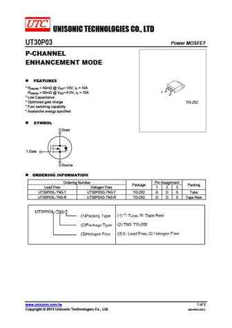
UNISONIC TECHNOLOGIES CO., LTD UT30P03 Power MOSFET P-CHANNEL ENHANCEMENT MODE FEATURES * RDS(ON)
ut3006.pdf
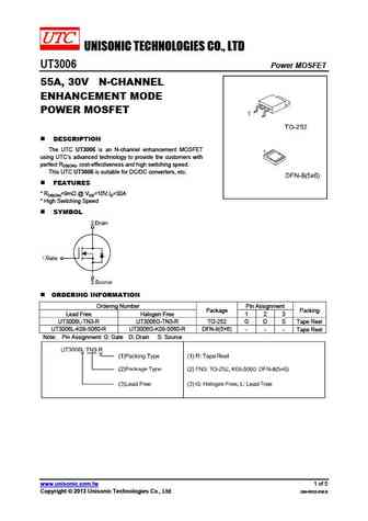
UNISONIC TECHNOLOGIES CO., LTD UT3006 Power MOSFET 55A, 30V N-CHANNEL ENHANCEMENT MODE POWER MOSFET DESCRIPTION The UTC UT3006 is an N-channel enhancement MOSFET using UTC s advanced technology to provide the customers with perfect RDS(ON), cost-effectiveness and high switching speed. This UTC UT3006 is suitable for DC/DC converters, etc. FEATURES * RDS(ON)
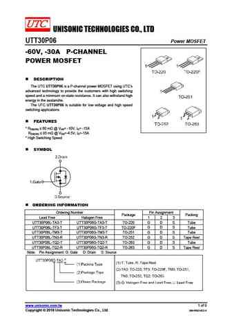
utt30p06l-ta3-t utt30p06g-ta3-t utt30p06l-tf3-t utt30p06g-tf3-t utt30p06l-tm3-t utt30p06g-tm3-t.pdf

UNISONIC TECHNOLOGIES CO., LTD UTT30P06 Power MOSFET -60V, -30A P-CHANNEL POWER MOSFET DESCRIPTION The UTC UTT30P06 is a P-channel power MOSFET using UTC s advanced technology to provide the customers with high switching speed and a minimum on-state resistance. It can also withstand high energy in the avalanche. The UTC UTT30P06 is suitable for low voltage and high speed
utt30p06.pdf
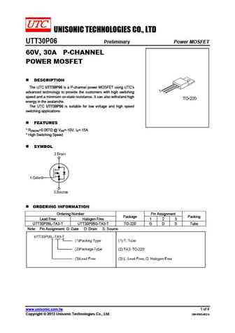
UNISONIC TECHNOLOGIES CO., LTD UTT30P06 Preliminary Power MOSFET 60V, 30A P-CHANNEL POWER MOSFET DESCRIPTION The UTC UTT30P06 is a P-channel power MOSFET using UTC s advanced technology to provide the customers with high switching speed and a minimum on-state resistance. It can also withstand high energy in the avalanche. The UTC UTT30P06 is suitable for low voltage and hi
utt30p04.pdf
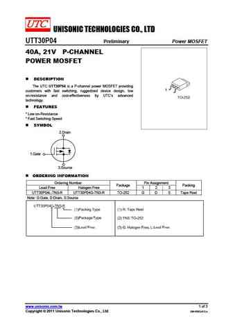
UNISONIC TECHNOLOGIES CO., LTD UTT30P04 Preliminary Power MOSFET 40A, 21V P-CHANNEL POWER MOSFET DESCRIPTION The UTC UTT30P04 is a P-channel power MOSFET providing customers with fast switching, ruggedized device design, low on-resistance and cost-effectiveness by UTC s advanced technology. FEATURES * Low on-Resistance * Fast Switching Speed SYMBOL 2.Drain 1.G
ut3055.pdf
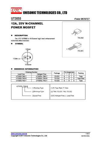
UNISONIC TECHNOLOGIES CO., LTD UT3055 Power MOSFET 12A, 25V N-CHANNEL POWER MOSFET 1 DESCRIPTION TO-252 The UTC UT3055 is N-Channel logic level enhancement mode field effect transistor. SYMBOL 2.Drain 1 TO-251 1.Gate 3.Source ORDERING INFORMATION Ordering Number Pin Assignment Package Packing Lead Free Halogen Free 1 2 3 UT3055-TM3-T UT3055L-TM3-T TO-251 G D
ut3009.pdf
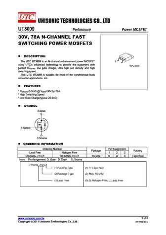
UNISONIC TECHNOLOGIES CO., LTD UT3009 Preliminary Power MOSFET 30V, 78A N-CHANNEL FAST SWITCHING POWER MOSFETS DESCRIPTION The UTC UT3009 is an N-channel enhancement power MOSFET using UTC s advanced technology to provide the customers with perfect RDS(ON), low gate charge, ultra high cell density and high switching speed. This UTC UT3009 is suitable for most of the synchr
ut30p04.pdf
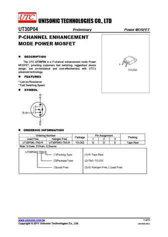
UNISONIC TECHNOLOGIES CO., LTD UT30P04 Preliminary Power MOSFET P-CHANNEL ENHANCEMENT MODE POWER MOSFET DESCRIPTION The UTC UT30P04 is a P-channel enhancement mode Power MOSFET, providing customers fast switching, ruggedized device design, low on-resistance and cost-effectiveness with UTC s advanced technology. FEATURES * Low on-Resistance * Fast Switching Speed
utt30n06.pdf

UNISONIC TECHNOLOGIES CO., LTD UTT30N06 Power MOSFET 30A, 60V N-CHANNEL POWER MOSFET DESCRIPTION The UTC UTT30N06 is a low voltage power MOSFET and is designed to have better characteristics, such as fast switching time, low gate charge, low on-state resistance and excellent avalanche characteristics. This power MOSFET is usually used in automotive applications of power suppl
utt30p06l-tq2-t utt30p06g-tq2-t utt30p06l-tq2-r utt30p06g-tq2-r utt30p06l-tn3-r utt30p06g-tn3-r.pdf
UNISONIC TECHNOLOGIES CO., LTD UTT30P06 Power MOSFET -60V, -30A P-CHANNEL POWER MOSFET DESCRIPTION The UTC UTT30P06 is a P-channel power MOSFET using UTC s advanced technology to provide the customers with high switching speed and a minimum on-state resistance. It can also withstand high energy in the avalanche. The UTC UTT30P06 is suitable for low voltage and high speed
utt30n10.pdf
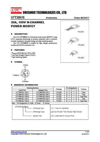
UNISONIC TECHNOLOGIES CO., LTD UTT30N10 Preliminary Power MOSFET 30A, 100V N-CHANNEL POWER MOSFET DESCRIPTION The UTC UTT30N10 is a N-channel mode power MOSFET using UTC s advanced technology to provide customers with a minimum on-state resistance, low gate charge and high switching speed. The UTC UTT30N10 is suitable for high voltage synchronous rectifier and DC/DC co
utt30n08.pdf
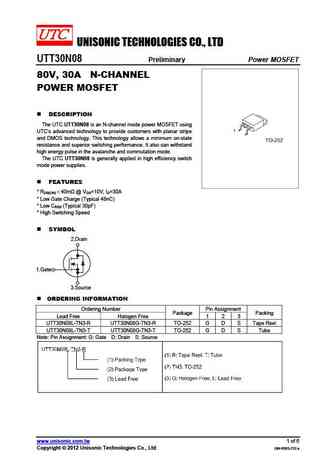
UNISONIC TECHNOLOGIES CO., LTD UTT30N08 Preliminary Power MOSFET 80V, 30A N-CHANNEL POWER MOSFET DESCRIPTION The UTC UTT30N08 is an N-channel mode power MOSFET using UTC s advanced technology to provide customers with planar stripe and DMOS technology. This technology allows a minimum on-state resistance and superior switching performance. It also can withstand high energy
apt30gn60bg.pdf

TYPICAL PERFORMANCE CURVES APT30GN60B(G) 600V APT30GN60B APT30GN60BG* *G Denotes RoHS Compliant, Pb Free Terminal Finish. Utilizing the latest Field Stop and Trench Gate technologies, these IGBT's have ultra low VCE(ON) and are ideal for low frequency applications that require absolute minimum conduction loss. Easy paralleling is a result of very tight parameter distribution and
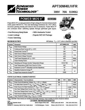
apt30m40b2vfrg.pdf
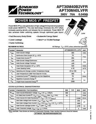
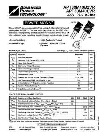
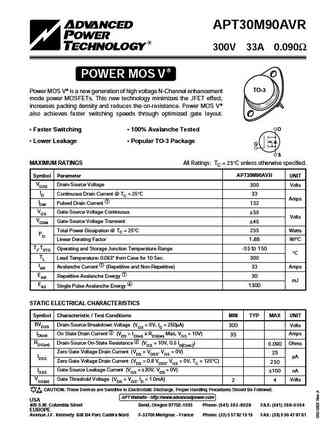
APT30M40B2VFR APT30M40LVFR 300V 76A 0.040 B2VFR POWER MOS V FREDFET T-MAX TO-264 Power MOS V is a new generation of high voltage N-Channel enhancement mode power MOSFETs. This new technology minimizes the JFET effect, increases packing density and reduces the on-resistance. Power MOS V also achieves faster switching speeds through optimized gate layout
apt30gf60ju3.pdf
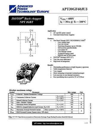
APT30GF60JU3 ISOTOP Buck chopper VCES = 600V IC = 30A @ Tc = 100 C NPT IGBT C Application AC and DC motor control Switched Mode Power Supplies G Features Non Punch Through (NPT) THUNDERBOLT IGBT - Low voltage drop - Low tail current E - Switching frequency up to 100 kHz - Soft recovery parallel diodes - Low diode VF - Low leakage current - Avalanch
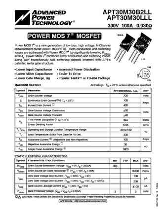
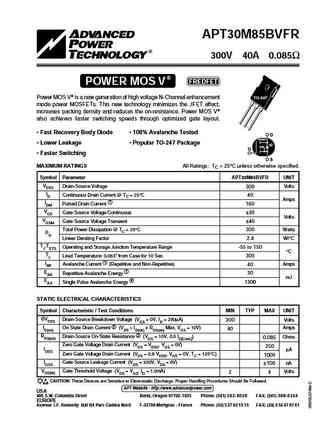
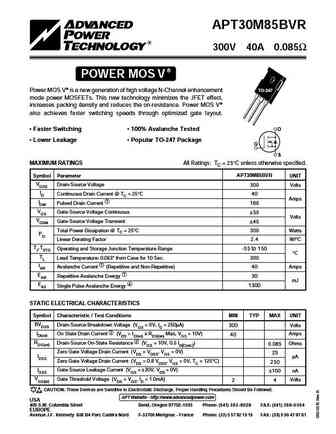
apt30m85.pdf

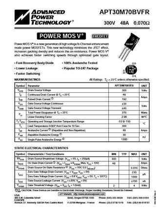
APT30M85BVFR 300V 40A 0.085 POWER MOS V FREDFET Power MOS V is a new generation of high voltage N-Channel enhancement TO-247 mode power MOSFETs. This new technology minimizes the JFET effect, increases packing density and reduces the on-resistance. Power MOS V also achieves faster switching speeds through optimized gate layout. Fast Recovery Body Diode 100% Avalanche Tes
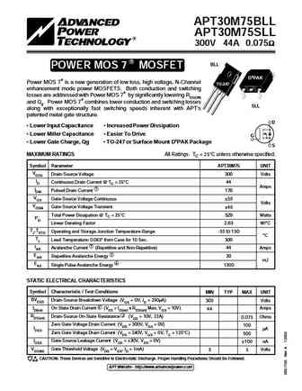
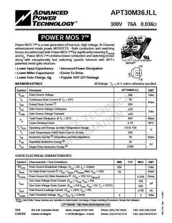
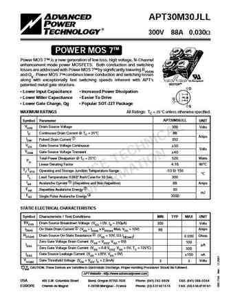
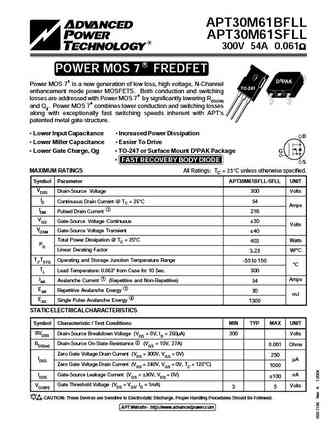
apt30m75bll.pdf

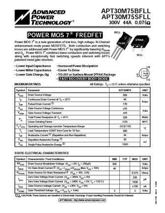
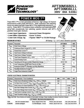
APT30M75BLL APT30M75SLL 300V 44A 0.075W TM BLL POWER MOS 7 Power MOS 7TM is a new generation of low loss, high voltage, N-Channel D3PAK TO-247 enhancement mode power MOSFETS. Both conduction and switching losses are addressed with Power MOS 7TM by significantly lowering RDS(ON) and Qg. Power MOS 7TM combines lower conduction and switching losses along with exceptionally fast switchin
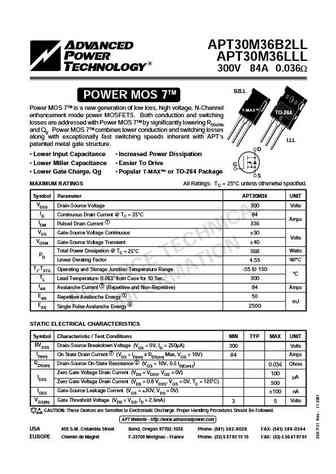
apt30m36b2fll apt30m36lfll.pdf
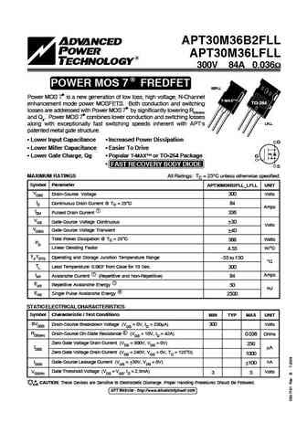
APT30M36B2FLL APT30M36LFLL 300V 84A 0.036 R FREDFET POWER MOS 7 FREDFET B2FLL Power MOS 7 is a new generation of low loss, high voltage, N-Channel T-MAX TO-264 enhancement mode power MOSFETS. Both conduction and switching losses are addressed with Power MOS 7 by significantly lowering RDS(ON) and Qg. Power MOS 7 combines lower conduction and switchin
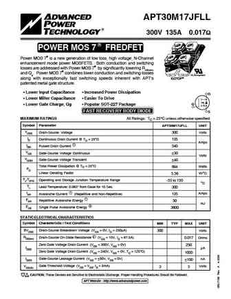
apt30m17jll.pdf
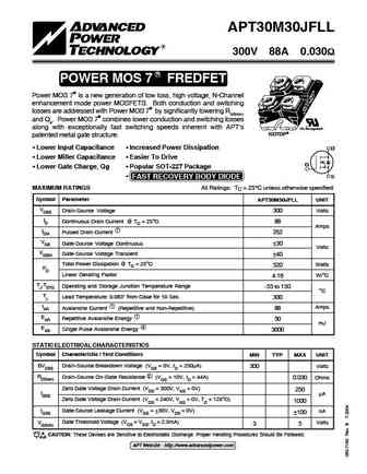
APT30M17JLL 300V 135A 0.017W TM POWER MOS 7 Power MOS 7TM is a new generation of low loss, high voltage, N-Channel enhancement mode power MOSFETS. Both conduction and switching losses are addressed with Power MOS 7TM by significantly lowering RDS(ON) and Qg. Power MOS 7TM combines lower conduction and switching losses along with exceptionally fast switching speeds inherent with APT's
apt30gn60bdq2g.pdf
TYPICAL PERFORMANCE CURVES APT30GN60BDQ2(G) 600V APT30GN60BDQ2 APT30GN60BDQ2G* *G Denotes RoHS Compliant, Pb Free Terminal Finish. Utilizing the latest Field Stop and Trench Gate technologies, these IGBT's have ultra low VCE(ON) and are ideal for low frequency applications that require absolute minimum conduction loss. Easy paralleling is a result of very tight parameter distrib
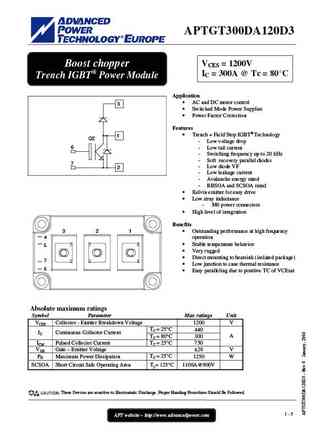
aptgt300a120d3.pdf

APTGT300A120D3 VCES = 1200V Phase Leg IC = 300A @ Tc = 80 C Trench IGBT Power Module Application Welding converters 3 Q1 Switched Mode Power Supplies 4 Uninterruptible Power Supplies Motor control 5 Features 1 Q2 Trench + Field Stop IGBT Technology 6 - Low voltage drop - Low tail current - Switching frequency up to 20 kHz 7 - Soft rec
aptgt30h170t3.pdf
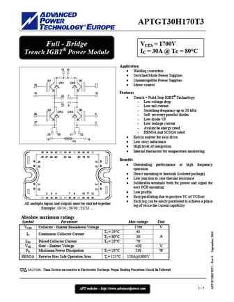
APTGT30H170T3 Full - Bridge VCES = 1700V IC = 30A @ Tc = 80 C Trench IGBT Power Module Application 13 14 Welding converters Switched Mode Power Supplies Q1 Q3 Uninterruptible Power Supplies CR1 CR3 11 18 Motor control Features 19 10 22 7 Trench + Field Stop IGBT Technology - Low voltage drop 23 8 - Low tail current Q2 Q4 - Switching fre
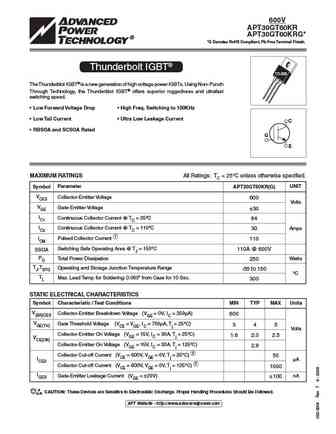
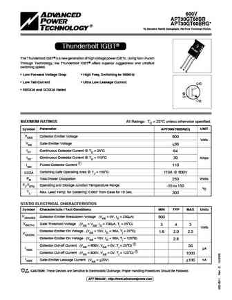
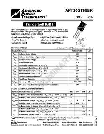
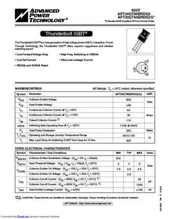
apt30gt60cr.pdf
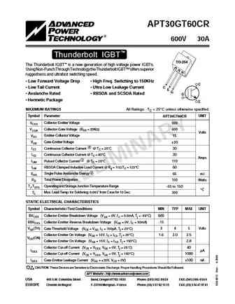
APT30GT60CR 600V 30A Thunderbolt IGBT TO-254 TO-254 The Thunderbolt IGBT is a new generation of high voltage power IGBTs. Using Non-Punch Through Technology the Thunderbolt IGBT offers superior ruggedness and ultrafast switching speed. Low Forward Voltage Drop High Freq. Switching to 150KHz C C Low Tail Current Ultra Low Leakage Current E G Avalanche R
apt30m75bfllg apt30m75sfllg.pdf
APT30M75BFLL APT30M75SFLL 300V 44A 0.075 BFLL R POWER MOS 7 FREDFET D3PAK Power MOS 7 is a new generation of low loss, high voltage, N-Channel TO-247 enhancement mode power MOSFETS. Both conduction and switching losses are addressed with Power MOS 7 by significantly lowering RDS(ON) and Qg. Power MOS 7 combines lower conduction and switching losses SFLL
aptgt300a170d3.pdf

APTGT300A170D3 VCES = 1700V Phase leg IC = 300A @ Tc = 80 C Trench IGBT Power Module Application Welding converters 3 Q1 Switched Mode Power Supplies Uninterruptible Power Supplies 4 Motor control 5 Features 1 Q2 Trench + Field Stop IGBT Technology - Low voltage drop 6 - Low tail current - Switching frequency up to 20 kHz 7 - Soft r
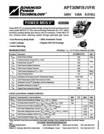
apt30m85svrg.pdf
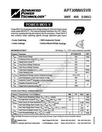
APT30M85SVR 300V 40A 0.085 POWER MOS V Power MOS V is a new generation of high voltage N-Channel enhancement D3PAK mode power MOSFETs. This new technology minimizes the JFET effect, increases packing density and reduces the on-resistance. Power MOS V also achieves faster switching speeds through optimized gate layout. Faster Switching 100% Avalanche Tested D Lower Lea
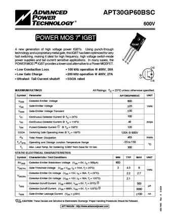
apt30gp60b.pdf
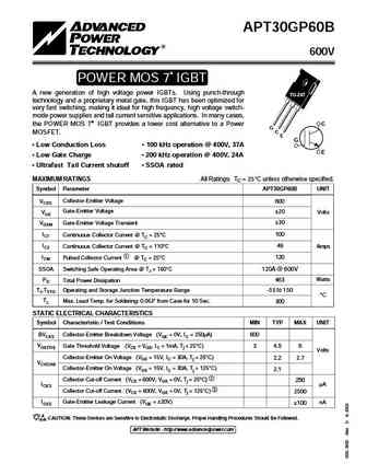
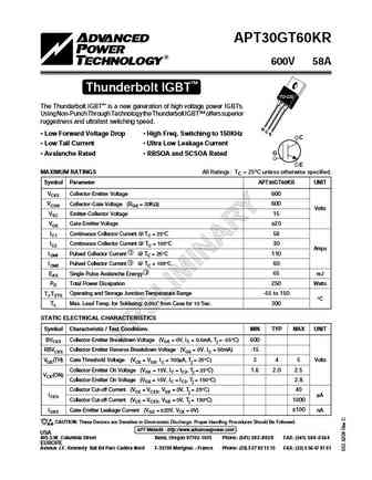
APT30GP60B 600V POWER MOS 7 IGBT A new generation of high voltage power IGBTs. Using punch-through TO-247 technology and a proprietary metal gate, this IGBT has been optimized for very fast switching, making it ideal for high frequency, high voltage switch- mode power supplies and tail current sensitive applications. In many cases, the POWER MOS 7 IGBT provides a lower cost alter
aptgt300u170d4.pdf

APTGT300U170D4 VCES = 1700V Single switch IC = 300A @ Tc = 80 C Trench IGBT Power Module Application Welding converters 1 Switched Mode Power Supplies Uninterruptible Power Supplies Motor control 3 Features Trench + Field Stop IGBT Technology 5 - Low voltage drop - Low tail current - Switching frequency up to 20 kHz 2 - Soft recovery pa
apt30gt60krg.pdf
TYPICAL PERFORMANCE CURVES APT30GT60KR(G) 600V APT30GT60KR APT30GT60KRG* *G Denotes RoHS Compliant, Pb Free Terminal Finish. Thunderbolt IGBT TO-220 The Thunderblot IGBT is a new generation of high voltage power IGBTs. Using Non- Punch Through Technology, the Thunderblot IGBT offers superior ruggedness and ultrafast switching speed. Low Forward Voltage Drop High
apt30gp60bdf1.pdf

TYPICAL PERFORMANCE CURVES APT30GP60BDF1 APT30GP60BDF1 600V POWER MOS 7 IGBT TO-247 A new generation of high voltage power IGBTs. Using punch-through technology and a proprietary metal gate, this IGBT has been optimized for very fast switching, making it ideal for high frequency, high voltage switch-mode G power supplies and tail current sensitive applications. In many cases, the
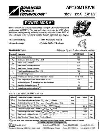
apt30m19jvfr.pdf
APT30M19JVFR 300V 130A 0.019 POWER MOS V FREDFET Power MOS V is a new generation of high voltage N-Channel enhancement mode power MOSFETs. This new technology minimizes the JFET effect, increases packing density and reduces the on-resistance. Power MOS V also achieves faster switching speeds through optimized gate layout. ISOTOP Fast Recovery Body Diode 100% Avalanche
aptgt300sk170d3.pdf

APTGT300SK170D3 VCES = 1700V Buck chopper IC = 300A @ Tc = 80 C Trench IGBT Power Module 3 Application Q1 AC and DC motor control 4 Switched Mode Power Supplies Features 5 1 Trench + Field Stop IGBT Technology - Low voltage drop - Low tail current - Switching frequency up to 20 kHz - Soft recovery parallel diodes 2 - Low diode VF - Low leakage
apt30m36jfll.pdf
APT30M36JFLL 300V 76A 0.036 R POWER MOS 7 FREDFET Power MOS 7 is a new generation of low loss, high voltage, N-Channel enhancement mode power MOSFETS. Both conduction and switching losses are addressed with Power MOS 7 by significantly lowering RDS(ON) "UL Recognized" and Qg. Power MOS 7 combines lower conduction and switching losses ISOTOP along with e
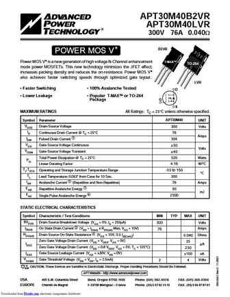
apt30m40b2vr.pdf
APT30M40B2VR APT30M40LVR 300V 76A 0.040W B2VR POWER MOS V T-MAX Power MOS V is a new generation of high voltage N-Channel enhancement TO-264 mode power MOSFETs. This new technology minimizes the JFET effect, increases packing density and reduces the on-resistance. Power MOS V also achieves faster switching speeds through optimized gate layout.. LVR Faster Switching
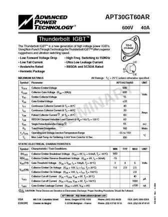
apt30gt60kr.pdf
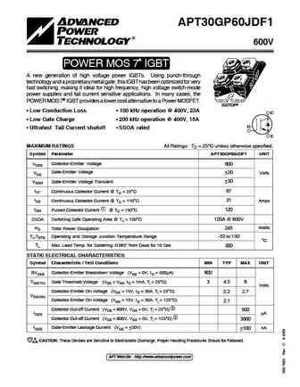
APT30GT60KR 600V 58A Thunderbolt IGBT TO-220 The Thunderbolt IGBT is a new generation of high voltage power IGBTs. Using Non-Punch Through Technology the Thunderbolt IGBT offers superior ruggedness and ultrafast switching speed. G C Low Forward Voltage Drop High Freq. Switching to 150KHz E C Low Tail Current Ultra Low Leakage Current Avalanche Rated
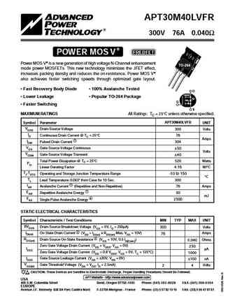
apt30m70bvr.pdf

APT30M70BVR 300V 48A 0.070 POWER MOS V Power MOS V is a new generation of high voltage N-Channel enhancement TO-247 mode power MOSFETs. This new technology minimizes the JFET effect, increases packing density and reduces the on-resistance. Power MOS V also achieves faster switching speeds through optimized gate layout. D Faster Switching 100% Avalanche Tested Lower
apt30gp60jdf1.pdf
TYPICAL PERFORMANCE CURVES APT30GP60JDF1 APT30GP60JDF1 600V POWER MOS 7 IGBT A new generation of high voltage power IGBTs. Using punch-through technology and a proprietary metal gate, this IGBT has been optimized for very fast switching, making it ideal for high frequency, high voltage switch-mode power supplies and tail current sensitive applications. In many cases, the "UL Recog
apt30gt60brd.pdf
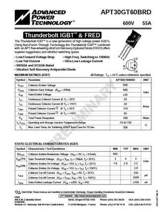
APT30GT60BRD 600V 55A Thunderbolt IGBT & FRED The Thunderbolt IGBT is a new generation of high voltage power IGBTs. TO-247 Using Non-Punch Through Technology the Thunderbolt IGBT combined with an APT free-wheeling ultraFast Recovery Epitaxial Diode (FRED) offers superior ruggedness and ultrafast switching speed. G Low Forward Voltage Drop High Freq. Switching to 150KHz
apt30m75bllg apt30m75sllg.pdf
APT30M75BLL APT30M75SLL 300V 44A 0.075 R BLL POWER MOS 7 MOSFET D3PAK Power MOS 7 is a new generation of low loss, high voltage, N-Channel TO-247 enhancement mode power MOSFETS. Both conduction and switching losses are addressed with Power MOS 7 by significantly lowering RDS(ON) and Qg. Power MOS 7 combines lower conduction and switching losses SLL alo
apt30m30b2llg apt30m30lllg.pdf
APT30M30B2LL APT30M30LLL 300V 100A 0.030 R B2LL POWER MOS 7 MOSFET T-MAX Power MOS 7 is a new generation of low loss, high voltage, N-Channel TO-264 enhancement mode power MOSFETS. Both conduction and switching losses are addressed with Power MOS 7 by significantly lowering RDS(ON) and Qg. Power MOS 7 combines lower conduction and switching losses LLL
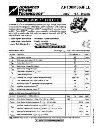
apt30m36jll.pdf
APT30M36JLL 300V 76A 0.036W TM POWER MOS 7 Power MOS 7TM is a new generation of low loss, high voltage, N-Channel enhancement mode power MOSFETS. Both conduction and switching losses are addressed with Power MOS 7TM by significantly lowering RDS(ON) and Qg. Power MOS 7TM combines lower conduction and switching losses along with exceptionally fast switching speeds inherent with APT's "
apt30m61bll.pdf

APT30M61BLL APT30M61SLL 300V 54A 0.061W TM BLL POWER MOS 7 Power MOS 7TM is a new generation of low loss, high voltage, N-Channel D3PAK TO-247 enhancement mode power MOSFETS. Both conduction and switching losses are addressed with Power MOS 7TM by significantly lowering RDS(ON) and Qg. Power MOS 7TM combines lower conduction and switching losses along with exceptionally fast switchin
apt30m85bvfr.pdf
APT30M85BVFR 300V 40A 0.085 POWER MOS V FREDFET Power MOS V is a new generation of high voltage N-Channel enhancement TO-247 mode power MOSFETs. This new technology minimizes the JFET effect, increases packing density and reduces the on-resistance. Power MOS V also achieves faster switching speeds through optimized gate layout. Fast Recovery Body Diode 100% Avalanche Tes
aptgt30a170d1.pdf

APTGT30A170D1 VCES = 1700V Phase leg IC = 30A @ Tc = 80 C Trench IGBT Power Module Application Welding converters 3 Q1 Switched Mode Power Supplies Uninterruptible Power Supplies 4 Motor control 5 Features 1 Q2 Trench + Field Stop IGBT Technology - Low voltage drop 6 - Low tail current - Switching frequency up to 20 kHz 7 - Soft rec
aptgt300u120d4.pdf

APTGT300U120D4 VCES = 1200V Single switch IC = 300A @ Tc = 80 C Trench IGBT Power Module Application Welding converters 1 Switched Mode Power Supplies Uninterruptible Power Supplies Motor control 3 Features Trench + Field Stop IGBT Technology 5 - Low voltage drop - Low tail current 2 - Switching frequency up to 20 kHz - Soft recovery p
apt30m85bvr.pdf
APT30M85BVR 300V 40A 0.085 POWER MOS V Power MOS V is a new generation of high voltage N-Channel enhancement TO-247 mode power MOSFETs. This new technology minimizes the JFET effect, increases packing density and reduces the on-resistance. Power MOS V also achieves faster switching speeds through optimized gate layout. Faster Switching 100% Avalanche Tested D Lower
apt30m36lll apt30m36b2ll.pdf
APT30M36B2LL APT30M36LLL 300V 84A 0.036W B2LL TM POWER MOS 7 Power MOS 7TM is a new generation of low loss, high voltage, N-Channel T-MAX TO-264 enhancement mode power MOSFETS. Both conduction and switching losses are addressed with Power MOS 7TM by significantly lowering RDS(ON) and Qg. Power MOS 7TM combines lower conduction and switching losses along with exceptionally fast s
apt30m40jvr.pdf

APT30M40JVR 300V 70A 0.040 POWER MOS V Power MOS V is a new generation of high voltage N-Channel enhancement mode power MOSFETs. This new technology minimizes the JFET effect, increases packing density and reduces the on-resistance. Power MOS V also achieves faster switching speeds through optimized gate layout. "UL Recognized" ISOTOP D Faster Switching 100% Avalanc
apt30gf60ju2.pdf
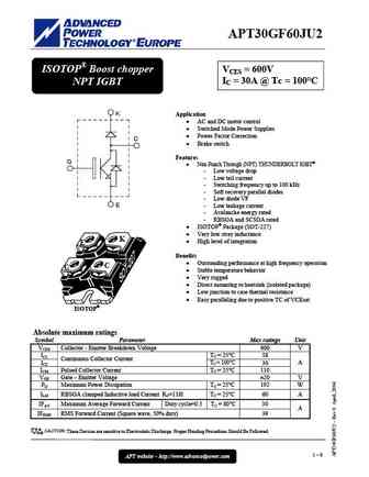
APT30GF60JU2 ISOTOP Boost chopper VCES = 600V IC = 30A @ Tc = 100 C NPT IGBT K Application AC and DC motor control Switched Mode Power Supplies Power Factor Correction C Brake switch Features G Non Punch Through (NPT) THUNDERBOLT IGBT - Low voltage drop - Low tail current - Switching frequency up to 100 kHz - Soft recovery parallel diodes -
apt30m30jll.pdf
APT30M30JLL 300V 88A 0.030W TM POWER MOS 7 Power MOS 7TM is a new generation of low loss, high voltage, N-Channel enhancement mode power MOSFETS. Both conduction and switching losses are addressed with Power MOS 7TM by significantly lowering RDS(ON) and Qg. Power MOS 7TM combines lower conduction and switching losses along with exceptionally fast switching speeds inherent with APT's "
aptgt300da170d3.pdf

APTGT300DA170D3 VCES = 1700V Boost chopper IC = 300A @ Tc = 80 C Trench IGBT Power Module Application AC and DC motor control 3 Switched Mode Power Supplies Power Factor Correction Features Trench + Field Stop IGBT Technology 1 Q2 - Low voltage drop - Low tail current 6 - Switching frequency up to 20 kHz - Soft recovery parallel diodes 7 -
apt30m36b2ll.pdf
APT30M36B2LL APT30M36LLL 300V 84A 0.036W B2LL TM POWER MOS 7 Power MOS 7TM is a new generation of low loss, high voltage, N-Channel T-MAX TO-264 enhancement mode power MOSFETS. Both conduction and switching losses are addressed with Power MOS 7TM by significantly lowering RDS(ON) and Qg. Power MOS 7TM combines lower conduction and switching losses along with exceptionally fast s
apt30m70bvfr.pdf
APT30M70BVFR 300V 48A 0.070 POWER MOS V FREDFET Power MOS V is a new generation of high voltage N-Channel enhancement TO-247 mode power MOSFETs. This new technology minimizes the JFET effect, increases packing density and reduces the on-resistance. Power MOS V also achieves faster switching speeds through optimized gate layout. Fast Recovery Body Diode 100% Avalanche Tes
apt30m30b2ll.pdf

APT30M30B2LL APT30M30LLL 300V 100A 0.030W B2LL TM POWER MOS 7 Power MOS 7TM is a new generation of low loss, high voltage, N-Channel T-MAX TO-264 enhancement mode power MOSFETS. Both conduction and switching losses are addressed with Power MOS 7TM by significantly lowering RDS(ON) and Qg. Power MOS 7TM combines lower conduction and switching losses along with exceptionally fast
aptgt300sk120d3.pdf

APTGT300SK120D3 VCES = 1200V Buck chopper IC = 300A @ Tc = 80 C Trench IGBT Power Module Application 3 Q1 AC and DC motor control Switched Mode Power Supplies 4 Features 5 Trench + Field Stop IGBT Technology 1 - Low voltage drop - Low tail current - Switching frequency up to 20 kHz - Soft recovery parallel diodes - Low diode VF 2 - Low leakag
apt30m30jfll.pdf
APT30M30JFLL 300V 88A 0.030 R POWER MOS 7 FREDFET Power MOS 7 is a new generation of low loss, high voltage, N-Channel enhancement mode power MOSFETS. Both conduction and switching losses are addressed with Power MOS 7 by significantly lowering RDS(ON) and Qg. Power MOS 7 combines lower conduction and switching losses along with exceptionally fast switching
apt30gp60bdq1g.pdf
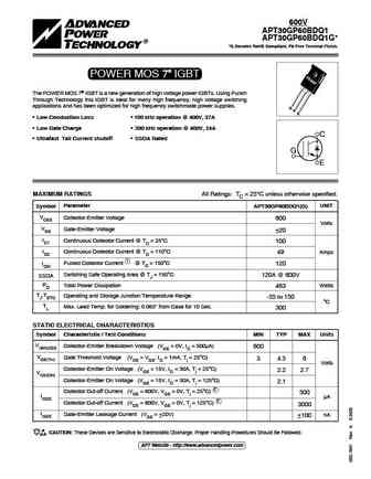
TYPICAL PERFORMANCE CURVES APT30GP60BDQ1(G) 600V APT30GP60BDQ1 APT30GP60BDQ1G* *G Denotes RoHS Compliant, Pb Free Terminal Finish. POWER MOS 7 IGBT The POWER MOS 7 IGBT is a new generation of high voltage power IGBTs. Using Punch Through Technology this IGBT is ideal for many high frequency, high voltage switching applications and has been optimized for high frequency swi
apt30m90avr.pdf
APT30M90AVR 300V 33A 0.090 POWER MOS V TO-3 Power MOS V is a new generation of high voltage N-Channel enhancement mode power MOSFETs. This new technology minimizes the JFET effect, increases packing density and reduces the on-resistance. Power MOS V also achieves faster switching speeds through optimized gate layout. D Faster Switching 100% Avalanche Tested Lower
aptgt30da170d1.pdf

APTGT30DA170D1 VCES = 1700V Boost chopper IC = 30A @ Tc = 80 C Trench IGBT Power Module Application AC and DC motor control 3 Switched Mode Power Supplies Power Factor Correction Features Trench + Field Stop IGBT Technology 1 Q2 - Low voltage drop - Low tail current 6 - Switching frequency up to 20 kHz - Soft recovery parallel diodes 7 - L
apt30gn60sg apt30gp60bg.pdf

APT30GP60B APT30GP60S 600V B POWER MOS 7 IGBT D3PAK A new generation of high voltage power IGBTs. Using punch-through technology and a proprietary metal gate, this IGBT has been optimized for S C very fast switching, making it ideal for high frequency, high voltage switch- G E mode power supplies and tail current sensitive applications. In many cases, the POWER MOS 7 IGBT pr
apt30gt60brg.pdf
TYPICAL PERFORMANCE CURVES APT30GT60BR(G) 600V APT30GT60BR APT30GT60BRG* *G Denotes RoHS Compliant, Pb Free Terminal Finish. Thunderbolt IGBT The Thunderblot IGBT is a new generation of high voltage power IGBTs. Using Non- Punch Through Technology, the Thunderblot IGBT offers superior ruggedness and ultrafast switching speed. G C E Low Forward Voltage Drop Hig
aptgt300da120d3.pdf
APTGT300DA120D3 VCES = 1200V Boost chopper IC = 300A @ Tc = 80 C Trench IGBT Power Module Application AC and DC motor control 3 Switched Mode Power Supplies Power Factor Correction Features Trench + Field Stop IGBT Technology 1 Q2 - Low voltage drop 6 - Low tail current - Switching frequency up to 20 kHz - Soft recovery parallel diodes 7 -
apt30m40b2vrg.pdf
APT30M40B2VR APT30M40LVR 300V 76A 0.040W B2VR POWER MOS V T-MAX Power MOS V is a new generation of high voltage N-Channel enhancement TO-264 mode power MOSFETs. This new technology minimizes the JFET effect, increases packing density and reduces the on-resistance. Power MOS V also achieves faster switching speeds through optimized gate layout.. LVR Faster Switching
apt30gt60br.pdf
APT30GT60BR 600V 58A Thunderbolt IGBT TO-247 The Thunderbolt IGBT is a new generation of high voltage power IGBTs. Using Non-Punch Through Technology the Thunderbolt IGBT offers superior ruggedness and ultrafast switching speed. G Low Forward Voltage Drop High Freq. Switching to 150KHz C C E Low Tail Current Ultra Low Leakage Current Avalanche Rated
aptgt30sk170d1.pdf

APTGT30SK170D1 VCES = 1700V Buck chopper IC = 30A @ Tc = 80 C Trench IGBT Power Module Application AC and DC motor control 3 Q1 Switched Mode Power Supplies 4 Features Trench + Field Stop IGBT Technology 5 - Low voltage drop 1 - Low tail current - Switching frequency up to 20 kHz - Soft recovery parallel diodes - Low diode VF - Low leakage cur
apt30m40lvfr.pdf
APT30M40LVFR 300V 76A 0.040 POWER MOS V FREDFET Power MOS V is a new generation of high voltage N-Channel enhancement TO-264 mode power MOSFETs. This new technology minimizes the JFET effect, increases packing density and reduces the on-resistance. Power MOS V also achieves faster switching speeds through optimized gate layout. Fast Recovery Body Diode 100% Avalanche Te
apt30m30b2fllg apt30m30lfll.pdf
APT30M30B2FLL APT30M30LFLL 300V 100A 0.030 R B2FLL POWER MOS 7 FREDFET T-MAX Power MOS 7 is a new generation of low loss, high voltage, N-Channel TO-264 enhancement mode power MOSFETS. Both conduction and switching losses are addressed with Power MOS 7 by significantly lowering RDS(ON) and Qg. Power MOS 7 combines lower conduction and switching losses
apt30gt60brdq2g.pdf
TYPICAL PERFORMANCE CURVES APT30GT60BRDQ2(G) 600V APT30GT60BRDQ2 APT30GT60BRDQ2G* *G Denotes RoHS Compliant, Pb Free Terminal Finish. Thunderbolt IGBT The Thunderblot IGBT is a new generation of high voltage power IGBTs. Using Non- Punch Through Technology, the Thunderblot IGBT offers superior ruggedness and ultrafast switching speed. G C E Low Forward Voltage Dro
apt30m61bfllg apt30m61sfllg.pdf
APT30M61BFLL APT30M61SFLL 300V 54A 0.061 R POWER MOS 7 FREDFET D3PAK Power MOS 7 is a new generation of low loss, high voltage, N-Channel TO-247 enhancement mode power MOSFETS. Both conduction and switching losses are addressed with Power MOS 7 by significantly lowering RDS(ON) and Qg. Power MOS 7 combines lower conduction and switching losses along with
apt30gp60bsc.pdf
TYPICAL PREFORMANCE CURVES APT30GP60BSC APT30GP60BSC 600V POWER MOS 7 IGBT TO-247 A new generation of high voltage power IGBTs. Using punch-through technology and a proprietary metal gate, this IGBT has been optimized for very fast switching, making it ideal for high frequency, high voltage switch-mode G power supplies and tail current sensitive applications. In many cases, the C
apt30m19jvr.pdf
APT30M19JVR 300V 130A 0.019 POWER MOS V Power MOS V is a new generation of high voltage N-Channel enhancement mode power MOSFETs. This new technology minimizes the JFET effect, increases packing density and reduces the on-resistance. Power MOS V also achieves faster switching speeds through optimized gate layout. "UL Recognized" ISOTOP Faster Switching 100% Avalanche
apt30m17jfll.pdf
APT30M17JFLL 300V 135A 0.017 R POWER MOS 7 FREDFET Power MOS 7 is a new generation of low loss, high voltage, N-Channel enhancement mode power MOSFETS. Both conduction and switching losses are addressed with Power MOS 7 by significantly lowering RDS(ON) and Qg. Power MOS 7 combines lower conduction and switching losses "UL Recognized" along with exceptiona
rft3055le.pdf
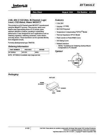
RFT3055LE Data Sheet August 1999 File Number 4537.3 2.0A, 60V, 0.150 Ohm, N-Channel, Logic Features Level, ESD Rated, Power MOSFET 2.0A, 60V This product is an N-Channel power MOSFET manufactured rDS(ON) = 0.150 using the MegaFET process. This process, which uses 2kV ESD Protected feature sizes approaching those of LSI circuits, gives optimum utilization of silicon, res
ct30vm-8.pdf
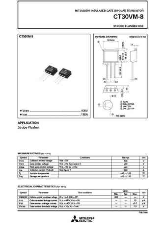
MITSUBISHI INSULATED GATE BIPOLAR TRANSISTOR CT30VM-8 STROBE FLASHER USE CT30VM-8 OUTLINE DRAWING Dimensions in mm 10.5MAX. r 1.3 1 0.5 0.5 2.5 2.5 q w e wr q GATE q w COLLECTOR e EMITTER r COLLECTOR VCES ................................................................................400V e ICM ...............................................................................
ct30tm-8.pdf
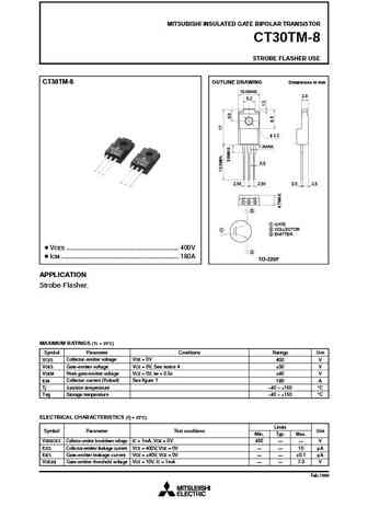
MITSUBISHI INSULATED GATE BIPOLAR TRANSISTOR CT30TM-8 STROBE FLASHER USE CT30TM-8 OUTLINE DRAWING Dimensions in mm 10.5MAX. 2.8 5.2 3.2 1.3MAX. 0.8 2.54 2.54 0.5 2.6 qwe w q GATE q w COLLECTOR e EMITTER VCES ............................................................................... 400V e ICM .........................................................................
ct30vs-8.pdf
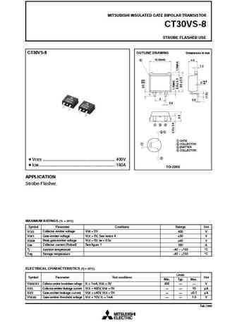
MITSUBISHI INSULATED GATE BIPOLAR TRANSISTOR CT30VS-8 STROBE FLASHER USE CT30VS-8 OUTLINE DRAWING Dimensions in mm r 10.5MAX. 4.5 1.3 +0.3 0 0 1 5 0.5 0.8 q w e wr q GATE q w COLLECTOR e EMITTER r COLLECTOR e VCES ............................................................................... 400V ICM ...................................................................
ct30sm-12.pdf
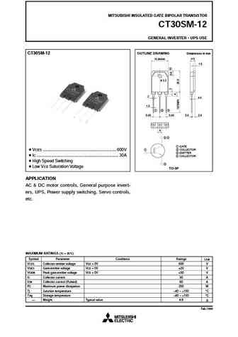
MITSUBISHI INSULATED GATE BIPOLAR TRANSISTOR CT30SM-12 GENERAL INVERTER UPS USE CT30SM-12 OUTLINE DRAWING Dimensions in mm 4.5 15.9MAX. 1.5 r 3.2 2 4.4 1.0 q w e 5.45 5.45 0.6 2.8 4 wr q GATE q w COLLECTOR VCES ................................................................................600V e EMITTER IC .........................................................
bft30csm.pdf
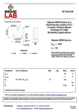
BFT30CSM Dimensions in mm (inches). Bipolar NPN Device in a 0.51 0.10 Hermetically sealed LCC1 (0.02 0.004) 0.31 rad. (0.012) Ceramic Surface Mount 3 Package for High Reliability Applications 21 1.91 0.10 (0.075 0.004) A 0.31 rad. Bipolar NPN Device. (0.012) 3.05 0.13 (0.12 0.005) 1.40 (0.055) 1.02 0.10 max. VCEO = 60V A = (0.04 0.004)
pzt3019.pdf
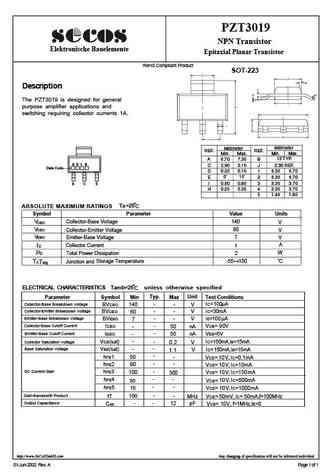
PZT3019 NPN Transistor Elektronische Bauelemente Epitaxial Planar Transistor RoHS Compliant Product SOT-223 Description The PZT3019 is designed for general purpose amplifier applications and switching requiring collector currents 1A. Millimeter Millimeter REF. REF. Min. Max. Min. Max. A 6.70 7.30 B 13 TYP. 3 0 1 9 C 2.90 3.10 J 2.30 REF. Date Code D 0.02 0.10 1 6.30
mzt3055 mzt2955.pdf
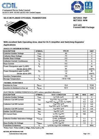
Continental Device India Limited An ISO/TS 16949, ISO 9001 and ISO 14001 Certified Company SILICON PLANAR EPITAXIAL TRANSISTORS MZT2955 PNP MZT3055 NPN SOT-223 Formed SMD Package With excellent Safe Operating Area, ideal for Hi-Fi Amplifier and Switching Regulator Applications ABSOLUTE MAXIMUM RATINGS DESCRIPTION SYMBOL VALUE UNIT Collector Emitter Voltage VCEO 60 V VCBO Collector
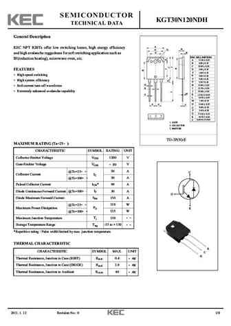
kgt30n135ndh.pdf
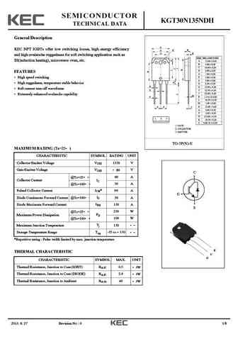
SEMICONDUCTOR KGT30N135NDH TECHNICAL DATA General Description KEC NPT IGBTs offer low switching losses, high energy efficiency and high avalanche ruggedness for soft switching application such as IH(induction heating), microwave oven, etc. FEATURES High speed switching High ruggedness, temperature stable behavior Soft current turn-off waveforms Extremely enhanced avalanche c
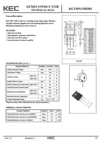
kgt30n135kdh.pdf
SEMICONDUCTOR KGT30N135KDH TECHNICAL DATA General Description B KEC NPT IGBTs offer low switching losses, high energy efficiency A O S K and high avalanche ruggedness for soft switching application such as IH(induction heating), microwave oven, etc. DIM MILLIMETERS _ + A 15.90 0.30 FEATURES _ B 5.00 + 0.20 High speed switching _ C 20.85 + 0.30 _ D 3.00 + 0.20 High r
kgt30n120ndh.pdf
SEMICONDUCTOR KGT30N120NDH TECHNICAL DATA General Description A KEC NPT IGBTs offer low switching losses, high energy efficiency Q B N O K and high avalanche ruggedness for soft switching application such as DIM MILLIMETERS IH(induction heating), microwave oven, etc. _ A + 15.60 0.20 _ B 4.80 + 0.20 _ C 19.90 + 0.20 _ D 2.00 0.20 FEATURES + _ d + 1.00 0.20 High speed
kgt30n120nda.pdf
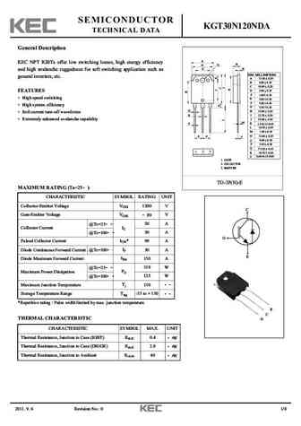
SEMICONDUCTOR KGT30N120NDA TECHNICAL DATA General Description A KEC NPT IGBTs offer low switching losses, high energy efficiency Q B N O K and high avalanche ruggedness for soft switching application such as DIM MILLIMETERS general inverters, etc. _ A + 15.60 0.20 _ B 4.80 + 0.20 _ C 19.90 + 0.20 _ D 2.00 0.20 FEATURES + _ d + 1.00 0.20 High speed switching _ E 3.
kgt30n60kda.pdf
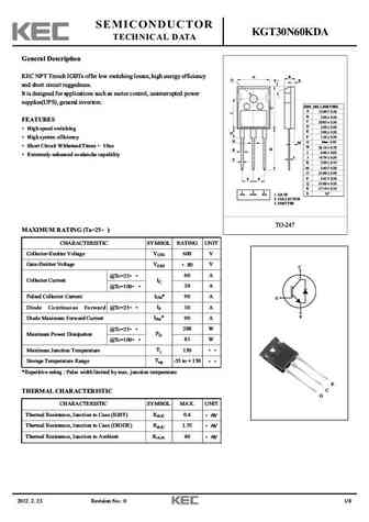
SEMICONDUCTOR KGT30N60KDA TECHNICAL DATA General Description KEC NPT Trench IGBTs offer low switching losses, high energy efficiency B A O S K and short circuit ruggedness. It is designed for applications such as motor control, uninterrupted power supplies(UPS), general inverters. DIM MILLIMETERS _ + A 15.90 0.30 _ B 5.00 + 0.20 FEATURES _ C 20.85 + 0.30 _ D 3.00 + 0.20
apt30f50b apt30f50s.pdf
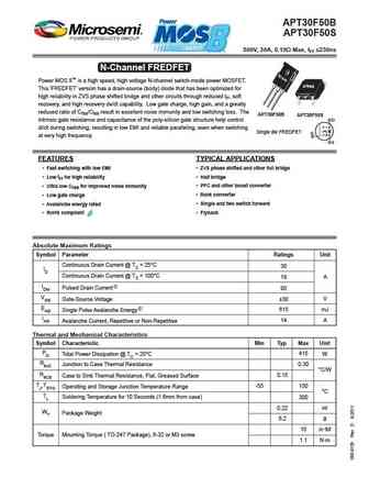
APT30F50B APT30F50S 500V, 30A, 0.19 Max, trr 230ns N-Channel FREDFET Power MOS 8 is a high speed, high voltage N-channel switch-mode power MOSFET. D3PAK This 'FREDFET' version has a drain-source (body) diode that has been optimized for high reliability in ZVS phase shifted bridge and other circuits through reduced trr, soft recovery, and high recovery dv/dt capability. Lo
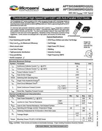
apt30gs60srdq2g.pdf
APT30GS60BRDQ2(G) APT30GS60SRDQ2(G) 600V, 30A, VCE(ON) = 2.8V Typical Thunderbolt High Speed NPT IGBT with Anti-Parallel 'DQ' Diode The Thunderbolt HS series is based on thin wafer non-punch through (NPT) technology similar to the Thunderbolt series, but trades higher VCE(ON) for significantly lower turn-on energy Eoff. The low switching losses enable operation at switching frequ
apt30gs60brdq2g.pdf

APT30GS60BRDQ2(G) APT30GS60SRDQ2(G) 600V, 30A, VCE(ON) = 2.8V Typical Thunderbolt High Speed NPT IGBT with Anti-Parallel 'DQ' Diode The Thunderbolt HS series is based on thin wafer non-punch through (NPT) technology similar to the Thunderbolt series, but trades higher VCE(ON) for significantly lower turn-on energy Eoff. The low switching losses enable operation at switching frequ
apt30gn60kg.pdf
TYPICAL PERFORMANCE CURVES APT30GN60K(G) 600V APT30GN60K APT30GN60KG* *G Denotes RoHS Compliant, Pb Free Terminal Finish. Utilizing the latest Field Stop and Trench Gate technologies, these IGBT's have ultra low VCE(ON) and are ideal for low frequency applications that require absolute minimum conduction loss. Easy paralleling is a result of very tight parameter distribution and a
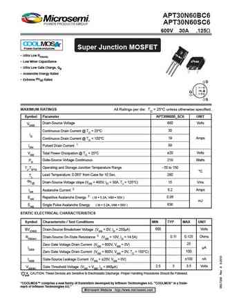
apt30n60bc6 apt30n60sc6.pdf
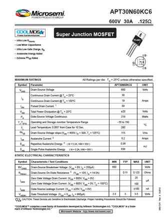
APT30N60BC6 APT30N60SC6 600V 30A .125 COOLMOS Power Semiconductors Super Junction MOSFET Ultra Low RDS(ON) D3PAK Low Miller Capacitance Ultra Low Gate Charge, Qg Avalanche Energy Rated Extreme dv/dt Rated D G S MAXIMUM RATINGS All Ratings per die TC = 25 C unless otherwise specified. Symbol Parameter APT30N60B_SC6 UNIT 600 Volts VDSS Drain-Sour
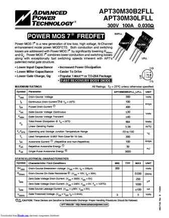
apt30m60j.pdf

APT30M60J 600V, 31A, 0.15 Max N-Channel MOSFET Power MOS 8 is a high speed, high voltage N-channel switch-mode power MOSFET. A proprietary planar stripe design yields excellent reliability and manufacturability. Low switching loss is achieved with low input capacitance and ultra low Crss "Miller" capaci- tance. The intrinsic gate resistance and capacitance of the poly-silicon ga
apt30f60j.pdf
APT30F60J 600V, 31A, 0.15 Max, trr 270ns N-Channel FREDFET Power MOS 8 is a high speed, high voltage N-channel switch-mode power MOSFET. This 'FREDFET' version has a drain-source (body) diode that has been optimized for high reliability in ZVS phase shifted bridge and other circuits through reduced trr, soft recovery, and high recovery dv/dt capability. Low gate charge, high
apt30n60kc6.pdf
APT30N60KC6 600V 30A .125 COOLMOS Power Semiconductors Super Junction MOSFET TO-220 Ultra Low RDS(ON) Low Miller Capacitance Ultra Low Gate Charge, Qg Avalanche Energy Rated D Extreme dv/dt Rated G S MAXIMUM RATINGS All Ratings per die TC = 25 C unless otherwise specified. Symbol Parameter APT30N60KC6 UNIT 600 Volts VDSS Drain-Source Voltage 30
apt30gt60brdlg.pdf
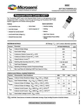
TYPICAL PERFORMANCE CURVES APT30GT60BRDL(G) 600V APT30GT60BRDL(G) *G Denotes RoHS Compliant, Pb Free Terminal Finish. Resonant Mode Combi IGBT The Thunderbolt IGBT used in this Resonant Mode Combi is a new generation of high voltage power IGBTs. Using Non- Punch Through Technology, the Thunderblot IGBT offers superior ruggedness and ultrafast switching speed. Typical Applicatio
j308 j309 j310 sst308 sst310 sst309 u309 u310.pdf
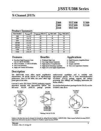
J/SST/U308 Series N-Channel JFETs J308 SST308 U309 J309 SST309 U310 J310 SST310 Product Summary Part Number VGS(off) (V) V(BR)GSS Min (V) gfs Min (mS) IDSS Min (mA) J308 1 to 6.5 25 8 12 J309 1 to 4 25 10 12 J310 2 to 6.5 25 8 24 SST308 1 to 6.5 25 8 12 SST309 1 to 4 25 10 12 SST310 2 to 6.5 25 8 24 U309 1 to 4 25 10 12
cet3055l.pdf
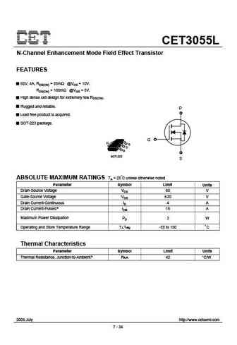
CET3055L N-Channel Enhancement Mode Field Effect Transistor FEATURES 60V, 4A, RDS(ON) = 85m @VGS = 10V. RDS(ON) = 100m @VGS = 5V. High dense cell design for extremely low RDS(ON). Rugged and reliable. D Lead free product is acquired. SOT-223 package. G D S D G SOT-223 S ABSOLUTE MAXIMUM RATINGS TA = 25 C unless otherwise noted Parameter Symbol Limit Units Drain-Source
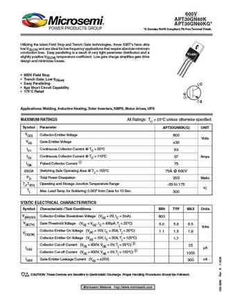
bt30n60anf.pdf
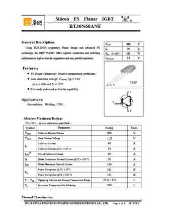
Silicon FS Planar IGBT R BT30N60ANF General Description VCES 600 V Using HUAJING's proprietary Planar design and advanced FS IC 30 A technology, the 600V FSIGBT offers superior conduction and switching Ptot TC=25 312 W performances, high avalanche ruggedness and easy parallel operation. VCE(SAT) 2.0 V Features FS Planar Technology, Positive temperature
kzt3055.pdf
SMD Type Transistors NPN Transistors CZT3055 (KZT3055) Unit mm SOT-223 6.50 0.2 3.00 0.1 Features 4 High Current Low Voltage Surface Mounted Power Amplifier Application 1 2 3 Complement to CZT2955 0.250 2.30 (typ) Gauge Plane 1.Base 2.Collector 0.70 0.1 3.Emitter 4.60 (typ) 4.Collector Absolute Maximum Ratings Ta = 25 Parameter Symbol
czt3055.pdf

SMD Type Transistors NPN Transistors CZT3055 (KZT3055) Unit mm SOT-223 6.50 0.2 3.00 0.1 Features 4 High Current Low Voltage Surface Mounted Power Amplifier Application 1 2 3 Complement to CZT2955 0.250 2.30 (typ) Gauge Plane 1.Base 2.Collector 0.70 0.1 3.Emitter 4.60 (typ) 4.Collector Absolute Maximum Ratings Ta = 25 Parameter Symbol
kdt3055l.pdf
SMD Type TrMOSFETs ansistor Unit mm SOT-223 6.50 0.2 3.00 0.1 4 1 2 3 D 0.250 2.30 (typ) 0.84 (max) Gauge Plane 0.66 (min) 1.Gate G D S 2.Drain 3.Source 4.60 (typ) 4.Drain 10 7.0 0.3 3.50 0.2 0.75 (min) 1.80 (max) 0.02 0.1 1.6 0.1 Mnsi E ors SMD Type TraOSFstT Mark ing Marking 3055L MOSFET SMD Type Transistors KDT3055L Typlacl Characteris
sgt30t60sdm1p7.pdf
SGT30T60SDM1P7 30A 600V C 2 SGT30T60SDM1P7 Field Stop III 1 G UPS SMPS PFC 3 E 30A 600V VCE sat =1.65V@IC=30
sgt30t60sd3pu.pdf
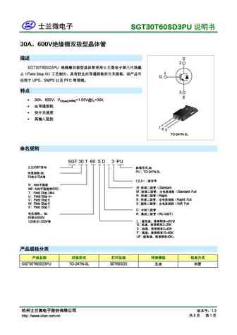
SGT30T60SD3PU 30A 600V C 2 SGT30T60SD3PU 1 Field Stop III G UPS SMPS PFC 3 E 30A 600V VCE(sat)( )=1.65V@IC=30A
art30u120.pdf
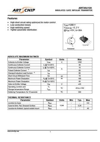
ART30U120 INSULATED GATE BIPOLAR TRANSISTOR Features High short circuit rating optimized for motor control Low conduction losses VCES=1200 V High switching speed VCE(on) typ. =3, 2 V Tighter parameter distribution @VGE =15V, Ic=30A N-channel ABSOLUTE MAXIMUM RATINGS Parameter Symbol Units Max Collector-to-Emitter Voltage VCES V 1200 Continuous Collector Cur
cht3055zgp.pdf
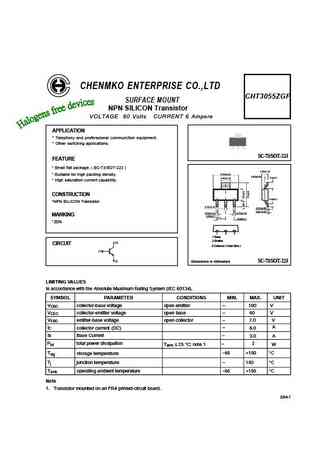
CHENMKO ENTERPRISE CO.,LTD CHT3055ZGP SURFACE MOUNT NPN SILICON Transistor VOLTAGE 60 Volts CURRENT 6 Ampere APPLICATION * Telephony and proferssional communction equipment. * Other switching applications. SC-73/SOT-223 FEATURE * Small flat package. ( SC-73/SOT-223 ) 1.65+0.15 6.50+0.20 * Suitable for high packing density. 0.90+0.05 2.0+0.3 3.00+0.10 * High saturation current
cht3019xgp.pdf
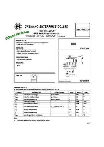
CHENMKO ENTERPRISE CO.,LTD CHT3019XGP SURFACE MOUNT NPN Switching Transistor VOLTAGE 80 Volts CURRENT 1 Ampere APPLICATION * Telephony and proferssional communction equipment. * Other switching applications. FEATURE SC-62/SOT-89 * Suitable for high packing density. * High saturation current capability. * Voltage controlled small signal switch. 4.6MAX. 1.6MAX. 1.7MAX. 0.4+0.05
cht3019gp.pdf
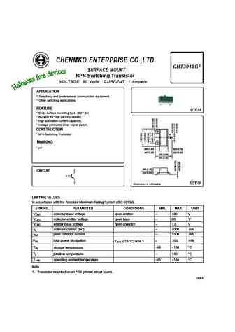
CHENMKO ENTERPRISE CO.,LTD CHT3019GP SURFACE MOUNT NPN Switching Transistor VOLTAGE 80 Volts CURRENT 1 Ampere APPLICATION * Telephony and proferssional communction equipment. * Other switching applications. FEATURE SOT-23 * Small surface mounting type. (SOT-23) * Suitable for high packing density. * High saturation current capability. * Voltage controlled small signal switch. (
cht3019zgp.pdf
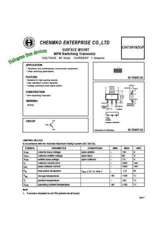
CHENMKO ENTERPRISE CO.,LTD CHT3019ZGP SURFACE MOUNT NPN Switching Transistor VOLTAGE 80 Volts CURRENT 1 Ampere APPLICATION * Telephony and proferssional communction equipment. * Other switching applications. FEATURE SC-73/SOT-223 * Suitable for high packing density. * High saturation current capability. 1.65+0.15 * Voltage controlled small signal switch. 6.50+0.20 0.90+0.05 2
ncep85t30ll.pdf
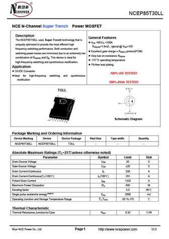
NCEP85T30LL NCE N-Channel Super Trench Power MOSFET Description General Features The NCEP85T30LL uses Super Trench technology that is VDS =85V,ID =330A uniquely optimized to provide the most efficient high RDS(ON)=1.6m , typical @ VGS=10V frequency switching performance. Both conduction and Excellent gate charge x RDS(on) product(FOM) switching power losses are min
ncep85t30t.pdf
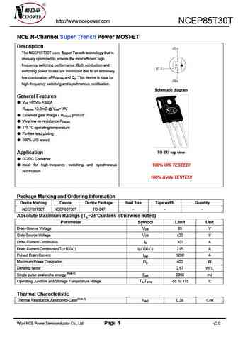
http //www.ncepower.com NCEP85T30T NCE N-Channel Super Trench Power MOSFET Description The NCEP85T30T uses Super Trench technology that is uniquely optimized to provide the most efficient high frequency switching performance. Both conduction and switching power losses are minimized due to an extremely low combination of RDS(ON) and Qg. This device is ideal for high-frequency sw
ncep01t30t.pdf
Pb Free Product http //www.ncepower.com NCEP01T30T NCE N-Channel Super Trench Power MOSFET Description The NCEP01T30T uses Super Trench technology that is uniquely optimized to provide the most efficient high frequency switching performance. Both conduction and switching power losses are minimized due to an extremely low combination of RDS(ON) and Qg. This device is ideal for hi
ncep40pt30vd.pdf
http //www.ncepower.com NCEP40PT30VD NCE P-Channel Super Trench Power MOSFET Description General Features The NCEP40PT30VD uses Super Trench technology that is V =-40V,I =-300A DS D uniquely optimized to provide the most efficient high R =1.6m , typical@ V =-10V DS(ON) GS frequency switching performance. Both conduction and R =2.2m , typical@ V =-4.5V DS(ON) GS switching p
ost30n65ktxf.pdf
OST30N65KTXF Enhancement Mode N-Channel Power IGBT General Description OST30N65KTXF uses advanced Oriental-Semi s patented Trident-Gate Bipolar Transistor (TGBTTM) technology to provide extremely low V (sat), low gate charge, and excellent switching CE performance. This device is suitable for mid to high range switching frequency converters. Features Advanced TGBTTM technol
ost30n65hmf.pdf
OST30N65HMF Enhancement Mode N-Channel Power IGBT General Description OST30N65HMF uses advanced Oriental-Semi s patented Trident-Gate Bipolar Transistor (TGBTTM) technology to provide extremely low V (sat), low gate charge, and excellent switching CE performance. This device is suitable for mid to high range switching frequency converters. Features Advanced TGBTTM technolog
ppmt30v3.pdf
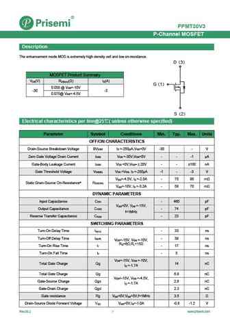
PPMT30V3 P-Channel MOSFET Description The enhancement mode MOS is extremely high density cell and low on-resistance. D 3 MOSFET Product Summary V (V) R ( ) I (A) DS DS(on) D G 1 0.058 @ V =-10V GS -30 -3 0.075@ V =-4.5V GS S 2 Electrical characteristics per line@25 ( unless otherwise specified) Parameter Symbol Conditions Min. Typ. Max. Units O
ppmt30v4.pdf
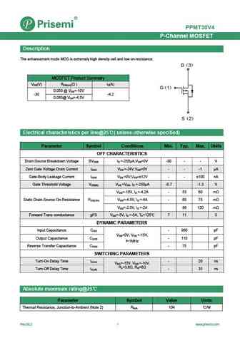
PPMT30V4 P-Channel MOSFET Description The enhancement mode MOS is extremely high density cell and low on-resistance. D 3 MOSFET Product Summary V (V) R ( ) I (A) DS DS(on) D G 1 0.053 @ V =-10V GS -30 -4.2 0.065@ V =-4.5V GS S 2 Electrical characteristics per line@25 ( unless otherwise specified) Parameter Symbol Conditions Min. Typ. Max. Units
pt236t30e2.pdf
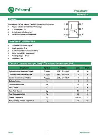
PT236T30E2 Transistor Feature 6 1 This device is Pb-Free, Halogen Free/BFR Free and RoHS compliant. Very low collector to emitter saturation voltage 5 2 DC current gain >100 3A continuous collector current 4 PNP epitaxial planar silicon transistor 3 Mechanical Characteristics Lead finish 100% matte Sn(Tin) Mounting position Any Qualified max reflow tem
pnm723t30v01.pdf

PNM723T30V01 N-Channel MOSFET Description PNM723T30V01 is designed for high speed switching applications The enhancement mode MOS is extremely high density cell and low on-resistance. D 3 MOSFET Product Summary V (V) R ( ) V (V) I (A) DS DS(on) GS(th) D 30 7@ V =2.5V,I =10mA 0.5 to 1.5 0.1 GS D G 1 S 2 Electrical characteristics per line@25 ( unless otherwise spec
pnmt30v6.pdf
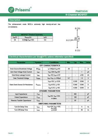
PNMT30V6 N-Channel MOSFET Description The enhancement mode MOS is extremely high density cell and low on-resistance. D 3 MOSFET Product Summary VDS(V) RDS(on)( ) ID(A) 30 0.030@ VGS=10V 5.8 G 1 S 2 Electrical characteristics per line@25 ( unless otherwise specified) Parameter Symbol Conditions Min. Typ. Max. Units OFF CHARACTERISTICS Drain-Source Br
pt236t30e2h.pdf
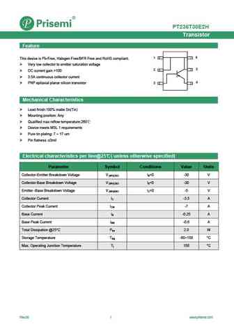
PT236T30E2H Transistor Feature 6 1 This device is Pb-Free, Halogen Free/BFR Free and RoHS compliant. Very low collector to emitter saturation voltage 5 2 DC current gain >100 3.5A continuous collector current 4 PNP epitaxial planar silicon transistor 3 Mechanical Characteristics Lead finish 100% matte Sn(Tin) Mounting position Any Qualifi
pnm523t30v01.pdf
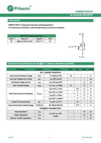
PNM523T30V01 N-Channel MOSFET Description PNM523T30V01 is designed for high speed switching applications The enhancement mode MOS is extremely high density cell and low on-resistance. D 3 MOSFET Product Summary V (V) R ( ) V (V) I (A) DS DS(on) GS(th) D 30 7@ V =2.5V,I =10mA 0.5 to 1.5 0.1 GS D G 1 S 2 Electrical characteristics per line@25 ( unless otherwise spec
pt236t30e2m.pdf
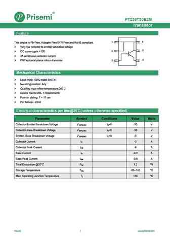
PT236T30E2M Transistor Feature 6 1 This device is Pb-Free, Halogen Free/BFR Free and RoHS compliant. Very low collector to emitter saturation voltage 5 2 DC current gain >100 3A continuous collector current 4 PNP epitaxial planar silicon transistor 3 Mechanical Characteristics Lead finish 100% matte Sn(Tin) Mounting position Any Qualified
ppt89t30v5ae2m.pdf
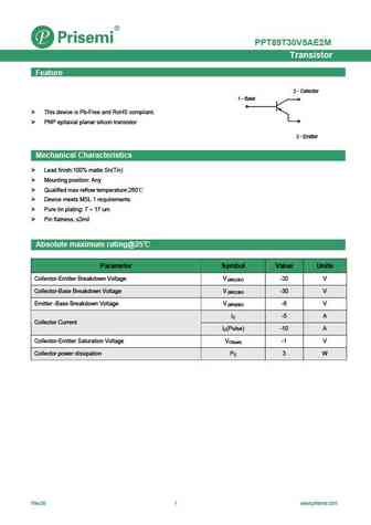
PPT89T30V5AE2M Transistor Feature 2 - Collector 1 - Base This device is Pb-Free and RoHS compliant. PNP epitaxial planar silicon transistor 3 - Emitter Mechanical Characteristics Lead finish 100% matte Sn(Tin) Mounting position Any Qualified max reflow temperature 260 Device meets MSL 1 requirements Pure tin plating 7 17 um Pin flatness 3m
bt30n60anf.pdf

Silicon FS Planar IGBT R BT30N60ANF General Description VCES 600 V Using HUAJING's proprietary Planar design and advanced FS IC 30 A technology, the 600V FSIGBT offers superior conduction and switching Ptot TC=25 312 W performances, high avalanche ruggedness and easy parallel operation. VCE(SAT) 2.0 V Features FS Planar Technology, Positive temperature
cst30n10f cst30n10u cst30n10d cst30n10p.pdf
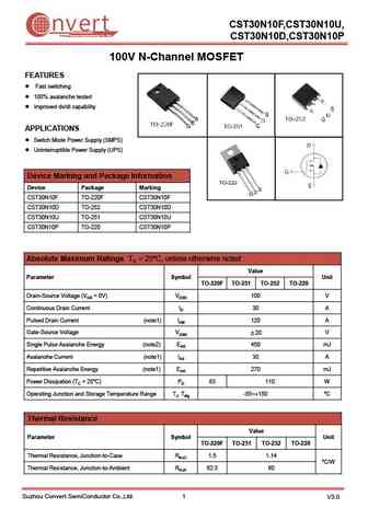
CST30N10F,CST30N10U, nvert Suzhou Convert Semiconductor Co ., Ltd. CST30N10D,CST30N10P 100V N-Channel MOSFET FEATURES Fast switching 100% avalanche tested Improved dv/dt capability APPLICATIONS Switch Mode Power Supply (SMPS) Uninterruptible Power Supply (UPS) Device Marking and Package Information Device Package Marking CST30N10F TO-220F CST30N10F CST30N10D T
fdz65t300d8g.pdf
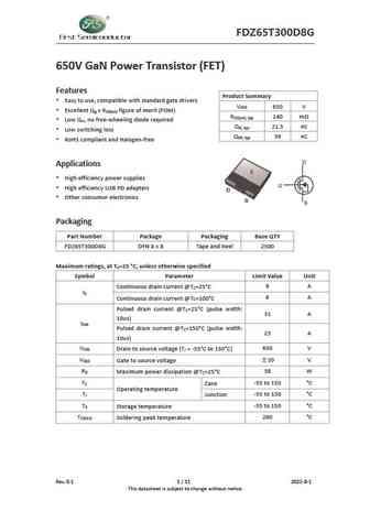
FDZ65T300D8G 650V GaN Power Transistor (FET) Features Product Summary Easy to use, compatible with standard gate drivers V 650 V DSS Excellent Q x R figure of merit (FOM) g DS(on) R 240 m DS(on), typ Low Q , no free-wheeling diode required rr Q 21.5 nC G, typ Low switching loss Q 39 nC RR, typ RoHS compliant and Halogen-free Applications S High eff
jjt30n65ss.pdf
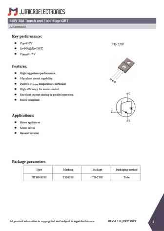
650V 30A Trench and Field Stop IGBT JJT30N65SS Key performance V =650V CE TO-220F I =30A@T =100 C C V =1.7 V CE(sat) Features High ruggedness performance. 10 s short circuit capability. G C E Positive V temperature coefficient. CE (sat) High efficiency for motor control. Excellent current sharing in parallel operation. RoHS compliant
jjt30n65ue.pdf
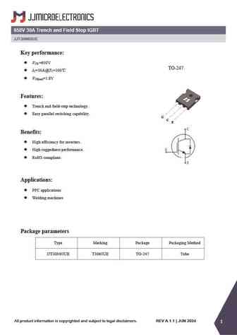
650V 30A Trench and Field Stop IGBT JJT30N65UE Key performance V =650V CE TO-247 I =30A@T =100 C C V =1.8V CE(sat) Features Trench and field-stop technology. Easy parallel switching capability. G C E Benefits High efficiency for inverters. High ruggedness performance. RoHS compliant. Applications PFC applications Welding machi
jjt30n65se.pdf
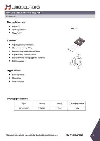
650V 30A Trench and Field Stop IGBT JJT30N65SE Key performance V =650V CE TO-247 I =30A@T =100 C C V =1.7 V CE(sat) Features High ruggedness performance. 10 s short circuit capability. G C Positive V temperature coefficient. CE (sat) E High efficiency for motor control. Excellent current sharing in parallel operation. RoHS compliant.
jjt30n65sy.pdf

650V 30A Trench and Field Stop IGBT JJT30N65SY Key performance TO-220 V =650V CE I =30A@T =100 C C V =1.7 V CE(sat) Features High ruggedness performance. G C 10 s short circuit capability. E Positive V temperature coefficient. CE (sat) High efficiency for motor control. Excellent current sharing in parallel operation. RoHS compliant.
agm13t30a.pdf
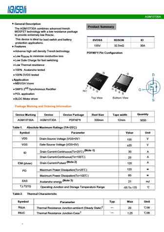
AGM13T30A Test Circuit 1) E test Circuit AS 2) Gate charge test Circuit 3) Switch Time Test Circuit www.agm-mos.com 3 VER2.55 AGM13T30A Typical Electrical and Thermal Characteristics Vds Drain-Source Voltage (V) T J-Junction Temperature( ) Figure 1 Output Characteristics Figure 4 Rdson-Junction Temperature Vgs Gate-Source Voltage (V) Qg Gate Charge (nC) Figure 2 Transfer Chara
agm13t30d.pdf
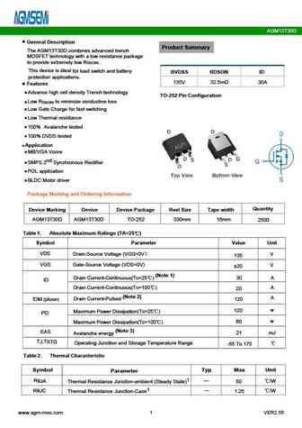
AGM13T30D General Description Product Summary The AGM13T30D combines advanced trench MOSFET technology with a low resistance package to provide extremely low R . DS(ON) This device is ideal for load switch and battery BVDSS RDSON ID protection applications. 135V 32.5m 30A Features Advance high cell density Trench technology TO-252 Pin Configuration Low R to m
wst3078.pdf
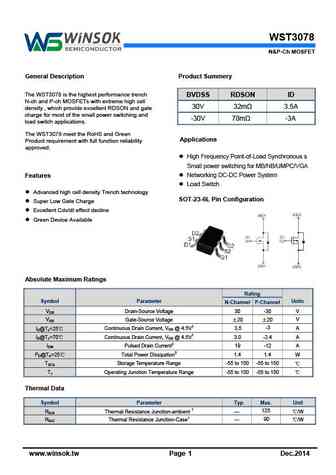
WST3078 N&P-Ch MOSFET General Description Product Summery The WST3078 is the highest performance trench BVDSS RDSON ID N-ch and P-ch MOSFETs with extreme high cell 30V 32m 3.5A density , which provide excellent RDSON and gate charge for most of the small power switching and -30V 78m -3A load switch applications. The WST3078 meet the RoHS and Green Applications Product
wst3052.pdf
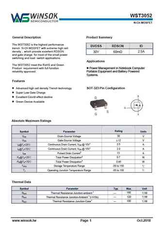
WST3052 N-Ch MOSFET General Description Product Summery The WST3052 is the highest performance BVDSS RDSON ID trench N-Ch MOSFET with extreme high cell density , which provide excellent RDSON 30V 60m 2.5A and gate charge for most of the small power switching and load switch applications. Applications The WST3052 meet the RoHS and Green Product requirement with full funct
wst3034.pdf
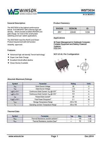
WST3034 N-Ch MOSFET General Description Product Summery The WST3034 is the highest performance BVDSS RDSON ID trench N-ch MOSFET with extreme high cell density , which provide excellent RDSON and 20V 22m 6.9A gate charge for most of the small power switching and load switch applications. Applications The WST3034 meet the RoHS and Green Product requirement with full functi
wst3032.pdf
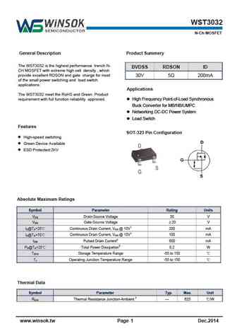
WST3032 N-Ch MOSFET General Description Product Summery The WST3032 is the highest performance trench N- BVDSS RDSON ID CH MOSFET with extreme high cell density , which provide excellent RDSON and gate charge for most 30V 5 200mA of the small power switching and load switch applications. Applications The WST3032 meet the RoHS and Green Product requirement with full functi
ndt3055.pdf

NDT3055 www.VBsemi.tw N-Channel 60-V (D-S) MOSFET FEATURES PRODUCT SUMMARY Halogen-free VDS (V) RDS(on) ( ) ID (A)a Qg (Typ.) TrenchFET Power MOSFET 0.076 at VGS = 10 V 4.5 RoHS 10 nC COMPLIANT 60 APPLICATIONS 0.085 at VGS = 4.5 V 3.5 Load Switches for Portable Devices D SOT-223-3 D G S D G S N-Channel MOSFET ABSOLUTE MAXIMUM RATINGS TA = 25 C, unless
ndt3055l.pdf
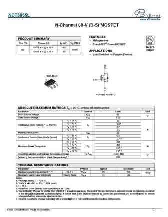
NDT3055L www.VBsemi.tw N-Channel 60-V (D-S) MOSFET FEATURES PRODUCT SUMMARY Halogen-free VDS (V) RDS(on) ( ) ID (A)a Qg (Typ.) TrenchFET Power MOSFET 0.076 at VGS = 10 V 4.5 RoHS 10 nC COMPLIANT 60 APPLICATIONS 0.085 at VGS = 4.5 V 3.5 Load Switches for Portable Devices D SOT-223-3 D G S D G S N-Channel MOSFET ABSOLUTE MAXIMUM RATINGS TA = 25 C, unless
ryu002n05t306.pdf
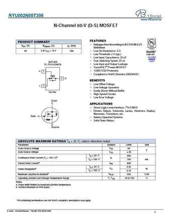
RYU002N05T306 www.VBsemi.tw N-Channel 60-V (D-S) MOSFET FEATURES PRODUCT SUMMARY Halogen-free According to IEC 61249-2-21 VDS (V) RDS(on) ( )ID (mA) Definition 2 at VGS = 10 V 60 300 Low On-Resistance 2 Low Threshold 2 V (typ.) Low Input Capacitance 25 pF Fast Switching Speed 25 ns SOT-323 Low Input and Output Leakage SC-70 (3-LEADS) TrenchF
hat3029r.pdf
HAT3029R www.VBsemi.tw N- and P-Channel 30 V (D-S) MOSFET FEATURES PRODUCT SUMMARY Halogen-free According to IEC 61249-2-21 VDS (V) RDS(on) ( ) Definition ID (A)a Qg (Typ.) TrenchFET Power MOSFET 0.018 at VGS = 10 V 8e 100 % Rg and UIS Tested N-Channel 30 0.020 at VGS = 8 V 8e 6.2 Compliant to RoHS Directive 2002/95/EC 0.024 at VGS = 4.5 V 8e 0.032 at VGS
vbgt30n135.pdf
VBGT30N135 www.VBsemi.com General Description VBsemi Field Stop Trench IGBTs offer low switching losses, high energy efficiency and high avalanche ruggedness for soft switching application such as IH(induction heating), microwave oven, etc. FEATURES High speed switching High ruggedness, temperature stable behavior Soft current turn-off waveforms Extremely enhanced avala
mmdt3052dw.pdf
MMDT3052DW ( NPN+NPN) Silicon Epitaxial Planar Transistor Features Each transistor elements are independent Applications For low frequency amplify application MARKING 5G Parameter Symbol Value Unit Collector Base Voltage VCBO 50 V Collector Emitter Voltage VCEO 50 V Emitter Base Voltage VEBO 6 V Collector Current IC 200 mA Power Dissipation Ptot 150 mW Junction Temperature
mdt30n06l.pdf
60V N-Channel Power MOSFET DESCRIPTION The MDT30N06L uses advanced trench technology to provide excellent RDS(ON), low gate charge. It can be used in a wide variety of applications. KEY CHARACTERISTICS VDS = 60V,ID= 30A RDS(ON)
mdt30p10d.pdf
MDT30P10D Silicon Silicon P-Channel Power MOSFET Description The MDT30P10D uses advanced technology and design to provide excellent RDS(ON) . It can be used in a wide variety of applications. General Features VDS=-110V, ID=-30A Low ON Resistance Low Reverse transfer capacitances 100% Single Pulse avalanche energy Test Application Power switching applicati
mdt30n10d mpg30n10p.pdf
100V N-Channel Power MOSFET DESCRIPTION The MPG30N10 uses advanced trench technology toprovide excellent R , low gate charge. It can be used in a wide DS(ON) variety of applications. KEY CHARACTERISTICS V = 100V,I =30A DS D R
mdt30n10.pdf

100V N-Channel Power MOSFET DESCRIPTION The MDT30N10 uses advanced trench technology to provide excellent R , low gate charge. It can be used DS(ON) in a wide variety of applications. KEY CHARACTERISTICS V = 100V,I = 30A R
apt30m36b2fll.pdf

isc N-Channel MOSFET Transistor APT30M36B2FLL FEATURES Drain Current I = 84A@ T =25 D C Drain Source Voltage- V =300V(Min) DSS Static Drain-Source On-Resistance R =0.036 (Max) DS(on) 100% avalanche tested Minimum Lot-to-Lot variations for robust device performance and reliable operation DESCRIPTION Designed for use in switch mode power supplies and general
apt30f50b.pdf

isc N-Channel MOSFET Transistor APT30F50B FEATURES Drain Current I = 30A@ T =25 D C Drain Source Voltage- V =500V(Min) DSS Static Drain-Source On-Resistance R = 0.19 (Max) DS(on) 100% avalanche tested Minimum Lot-to-Lot variations for robust device performance and reliable operation DESCRIPTION Designed for use in switch mode power supplies and general purp
apt30m75bll.pdf

isc N-Channel MOSFET Transistor APT30M75BLL FEATURES Drain Current I =44A@ T =25 D C Drain Source Voltage- V =300V(Min) DSS Static Drain-Source On-Resistance R =0.075 (Max) DS(on) 100% avalanche tested Minimum Lot-to-Lot variations for robust device performance and reliable operation DESCRIPTION Designed for use in switch mode power supplies and general pur
apt30m36lll.pdf
isc N-Channel MOSFET Transistor APT30M36LLL FEATURES Drain Current I = 84A@ T =25 D C Drain Source Voltage- V =300V(Min) DSS Static Drain-Source On-Resistance R =0.036 (Max) DS(on) 100% avalanche tested Minimum Lot-to-Lot variations for robust device performance and reliable operation DESCRIPTION Designed for use in switch mode power supplies and general pu
apt30m75bfll.pdf

isc N-Channel MOSFET Transistor APT30M75BFLL FEATURES Drain Current I = 44A@ T =25 D C Drain Source Voltage- V =300V(Min) DSS Static Drain-Source On-Resistance R =0.075 (Max) DS(on) 100% avalanche tested Minimum Lot-to-Lot variations for robust device performance and reliable operation DESCRIPTION Designed for use in switch mode power supplies and general p
apt30m70bvr.pdf

isc N-Channel MOSFET Transistor APT30M70BVR FEATURES Drain Current I =48A@ T =25 D C Drain Source Voltage- V =300V(Min) DSS Static Drain-Source On-Resistance R =0.07 (Max) DS(on) 100% avalanche tested Minimum Lot-to-Lot variations for robust device performance and reliable operation DESCRIPTION Designed for use in switch mode power supplies and general purp
apt30m30b2fll.pdf

isc N-Channel MOSFET Transistor APT30M30B2FLL FEATURES Drain Current I = 100A@ T =25 D C Drain Source Voltage- V =300V(Min) DSS Static Drain-Source On-Resistance R =0.03 (Max) DS(on) 100% avalanche tested Minimum Lot-to-Lot variations for robust device performance and reliable operation DESCRIPTION Designed for use in switch mode power supplies and general
apt30m36lfll.pdf

isc N-Channel MOSFET Transistor APT30M36LFLL FEATURES Drain Current I = 100A@ T =25 D C Drain Source Voltage- V =300V(Min) DSS Static Drain-Source On-Resistance R =0.03 (Max) DS(on) 100% avalanche tested Minimum Lot-to-Lot variations for robust device performance and reliable operation DESCRIPTION Designed for use in switch mode power supplies and general p
bdt30f af bf cf df.pdf
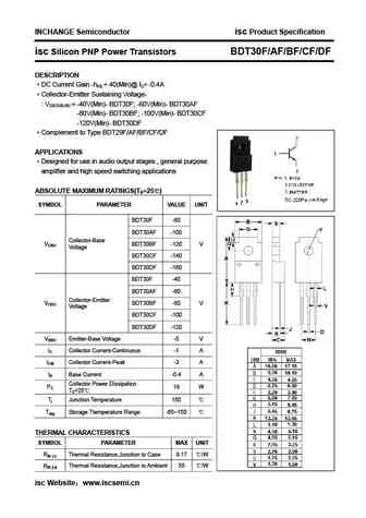
INCHANGE Semiconductor isc Product Specification isc Silicon PNP Power Transistors BDT30F/AF/BF/CF/DF DESCRIPTION DC Current Gain -hFE = 40(Min)@ IC= -0.4A Collector-Emitter Sustaining Voltage- VCEO(SUS) = -40V(Min)- BDT30F; -60V(Min)- BDT30AF -80V(Min)- BDT30BF; -100V(Min)- BDT30CF -120V(Min)- BDT30DF Complement to Type BDT29F/AF/BF/CF/DF APPLICATIONS Designed fo
apt30m30lfll.pdf

isc N-Channel MOSFET Transistor APT30M30LFLL FEATURES Drain Current I = 100A@ T =25 D C Drain Source Voltage- V =300V(Min) DSS Static Drain-Source On-Resistance R =0.03 (Max) DS(on) 100% avalanche tested Minimum Lot-to-Lot variations for robust device performance and reliable operation DESCRIPTION Designed for use in switch mode power supplies and general p
apt30m61bll.pdf

isc N-Channel MOSFET Transistor APT30M61BLL FEATURES Drain Current I =54A@ T =25 D C Drain Source Voltage- V =300V(Min) DSS Static Drain-Source On-Resistance R =0.061 (Max) DS(on) 100% avalanche tested Minimum Lot-to-Lot variations for robust device performance and reliable operation DESCRIPTION Designed for use in switch mode power supplies and general pur
apt30m61bfll.pdf

isc N-Channel MOSFET Transistor APT30M61BFLL FEATURES Drain Current I = 54A@ T =25 D C Drain Source Voltage- V =300V(Min) DSS Static Drain-Source On-Resistance R =0.061 (Max) DS(on) 100% avalanche tested Minimum Lot-to-Lot variations for robust device performance and reliable operation DESCRIPTION Designed for use in switch mode power supplies and general p
apt30m85bvr.pdf

isc N-Channel MOSFET Transistor APT30M85BVR FEATURES Drain Current I =40A@ T =25 D C Drain Source Voltage- V =300V(Min) DSS Static Drain-Source On-Resistance R =0.085 (Max) DS(on) 100% avalanche tested Minimum Lot-to-Lot variations for robust device performance and reliable operation DESCRIPTION Designed for use in switch mode power supplies and general pur
apt30n60bc6.pdf
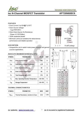
isc N-Channel MOSFET Transistor APT30N60BC6 FEATURES Drain Current I =30A@ T =25 D C Drain Source Voltage- V =600V(Min) DSS Static Drain-Source On-Resistance R =0.125 (Max) DS(on) 100% avalanche tested Minimum Lot-to-Lot variations for robust device performance and reliable operation DESCRIPTION Designed for use in switch mode power supplies and general pur
bdt30 a b c.pdf
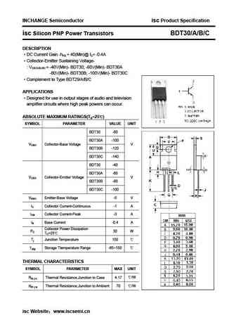
INCHANGE Semiconductor isc Product Specification isc Silicon PNP Power Transistors BDT30/A/B/C DESCRIPTION DC Current Gain -hFE = 40(Min)@ IC= -0.4A Collector-Emitter Sustaining Voltage- VCEO(SUS) = -40V(Min)- BDT30; -60V(Min)- BDT30A -80V(Min)- BDT30B; -100V(Min)- BDT30C Complement to Type BDT29/A/B/C APPLICATIONS Designed for use in output stages of audio and tele
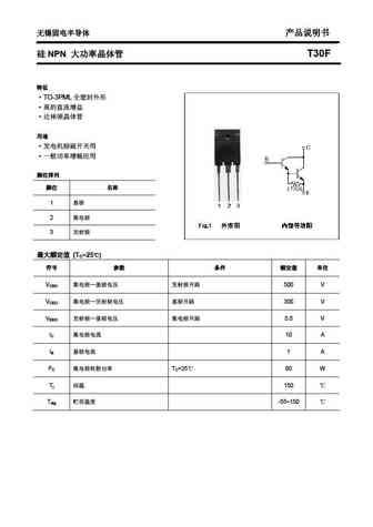
apt30m36b2ll.pdf

isc N-Channel MOSFET Transistor APT30M36B2LL FEATURES Drain Current I = 84A@ T =25 D C Drain Source Voltage- V =300V(Min) DSS Static Drain-Source On-Resistance R =0.036 (Max) DS(on) 100% avalanche tested Minimum Lot-to-Lot variations for robust device performance and reliable operation DESCRIPTION Designed for use in switch mode power supplies and general p
apt30m70bvfr.pdf
isc N-Channel MOSFET Transistor APT30M70BVFR FEATURES Drain Current I = 48A@ T =25 D C Drain Source Voltage- V =300V(Min) DSS Static Drain-Source On-Resistance R =0.07 (Max) DS(on) 100% avalanche tested Minimum Lot-to-Lot variations for robust device performance and reliable operation DESCRIPTION Designed for use in switch mode power supplies and general pu
apt30m30b2ll.pdf
isc N-Channel MOSFET Transistor APT30M30B2LL FEATURES Drain Current I = 100A@ T =25 D C Drain Source Voltage- V =300V(Min) DSS Static Drain-Source On-Resistance R =0.03 (Max) DS(on) 100% avalanche tested Minimum Lot-to-Lot variations for robust device performance and reliable operation DESCRIPTION Designed for use in switch mode power supplies and general p
bdt30f bdt30af bdt30bf bdt30cf bdt30df.pdf
isc Silicon PNP Power Transistors BDT30F/AF/BF/CF/DF DESCRIPTION DC Current Gain -h = 40(Min)@ I = -0.4A FE C Collector-Emitter Sustaining Voltage- V = -40V(Min)- BDT30F; -60V(Min)- BDT30AF CEO(SUS) -80V(Min)- BDT30BF; -100V(Min)- BDT30CF -120V(Min)- BDT30DF Complement to Type BDT29F/AF/BF/CF/DF Minimum Lot-to-Lot variations for robust device performance and reliable operat
sct3060.pdf
isc N-Channel SiC SMOSFET Transistor SCT3060 FEATURES Static drain-source on-resistance RDS(on) 78m Fast switching speed Fast reverse recovery 100% avalanche tested Minimum Lot-to-Lot variations for robust device performance and reliable operation DESCRITION DC/DC converters Switch mode power supplies ABSOLUTE MAXIMUM RATINGS(T =25 ) a SYMBOL PARAMETER
utt30n10.pdf
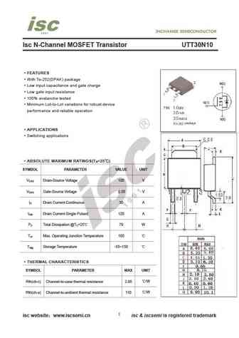
Isc N-Channel MOSFET Transistor UTT30N10 FEATURES With To-252(DPAK) package Low input capacitance and gate charge Low gate input resistance 100% avalanche tested Minimum Lot-to-Lot variations for robust device performance and reliable operation APPLICATIONS Switching applications ABSOLUTE MAXIMUM RATINGS(T =25 ) a SYMBOL PARAMETER VALUE UNIT V Drain-Source Volta
bdt30 bdt30a bdt30b bdt30c.pdf
isc Silicon PNP Power Transistors BDT30/A/B/C DESCRIPTION DC Current Gain -h = 40(Min)@ I = -0.4A FE C Collector-Emitter Sustaining Voltage- V = -40V(Min)- BDT30; -60V(Min)- BDT30A CEO(SUS) -80V(Min)- BDT30B; -100V(Min)- BDT30C Complement to Type BDT29/A/B/C Minimum Lot-to-Lot variations for robust device performance and reliable operation APPLICATIONS Designed for use i
Otros transistores... BUW13AW , BUW13W , T06 , T2141 , T2141F , T2142 , T2142F , T25 , 2SC945 , T30F , T430 , 2PD601AW , 2SA1235A , 2SA1586 , 2SA1797 , 2SB1132 , 2SB1188 .
History: 2S58 | 2S305
🌐 : EN ES РУ

Liste
Recientemente añadidas las descripciónes de los transistores:
BJT: GA1A4M | SBT42 | 2SA200-Y | 2SA200-O | 2SD882-Q | 2SD882-P | 2SD882-E | 2SC945-L | 2SC945-H | 2SC4226-R23 | 2SC3357-F | 2SC3357-E | 2SC3356-R26 | 2SC3356-R24 | 2SC3356-R23 | 2SB772-Q | 2SB772-P | 2SB772-E | 2SA1015-L | 2SA1015-H | HSS8550
Popular searches
mje15032g | irf1404 | bc550 | irf9530 | 2n2222a transistor | irfp250 | irf640n datasheet | irf540 datasheet