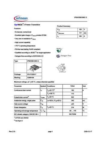
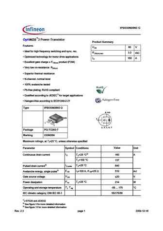
IPB030N08N3G Datasheet. Specs and Replacement
Type Designator: IPB030N08N3G 📄📄
Type of Transistor: MOSFET
Type of Control Channel: N-Channel
Absolute Maximum Ratings
Pd ⓘ - Maximum Power Dissipation: 214 W
|Vds|ⓘ - Maximum Drain-Source Voltage: 80 V
|Vgs|ⓘ - Maximum Gate-Source Voltage: 20 V
|Id| ⓘ - Maximum Drain Current: 160 A
Tj ⓘ - Maximum Junction Temperature: 175 °C
Electrical Characteristics
tr ⓘ - Rise Time: 79 nS
Cossⓘ - Output Capacitance: 1640 pF
RDSonⓘ - Maximum Drain-Source On-State Resistance: 0.003 Ohm
Package: TO263
📄📄 Copy
IPB030N08N3G substitution
- MOSFET ⓘ Cross-Reference Search
IPB030N08N3G datasheet
3.1. Size:696K infineon
ipb030n08n3.pdf 
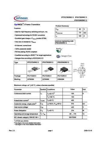
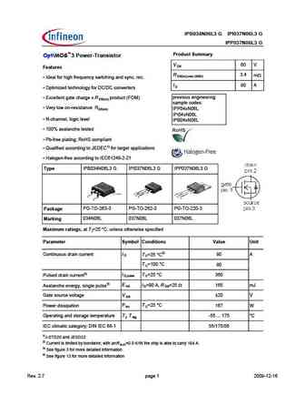
IPB030N08N3 G 3 Power-Transistor Product Summary Features V D Q #4513I CG9D389>7 1>4 CI>3 B53 R m D n) m x Q ( @D9=9J54 D538>?C I 1 D Q H35... See More ⇒
9.1. Size:475K infineon
ipb034n06l3g ipi037n06l3g ipp037n06l3g.pdf
Type IPB034N06L3 G IPI037N06L3 G IPP037N06L3 G Product Summary OptiMOS 3 Power-Transistor V 60 V DS Features R 3.4 m DS(on),max (SMD) Ideal for high frequency switching and sync. rec. I 90 A D Optimized technology for DC/DC converters previous engineering Excellent gate charge x R product (FOM) DS(on) sample codes Very low on-resistance RDS(on) IPP04xN06... See More ⇒
9.2. Size:674K infineon
ipb034n06n3.pdf
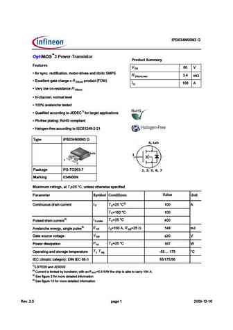
pe IPB034N06N3 G 3 Power-Transistor Product Summary Features V D P 6?A BH>3 A53C96931C9?> =?C?A 4A9E5B 1>4 43 43 ,&), R 4 m D n) m x P G35... See More ⇒
9.3. Size:264K infineon
ipp039n04lg ipb039n04lg.pdf
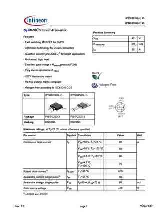
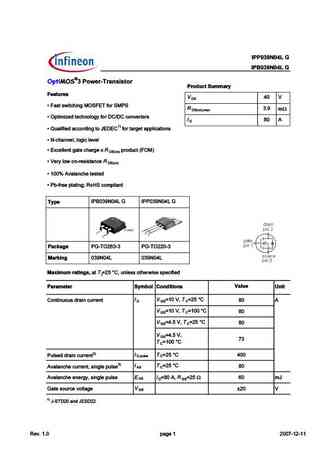
Type IPP039N04L G IPB039N04L G OptiMOS 3 Power-Transistor Product Summary Features V 40 V DS Fast switching MOSFET for SMPS R 3.9 m DS(on),max Optimized technology for DC/DC converters I 80 A D Qualified according to JEDEC1) for target applications N-channel, logic level Excellent gate charge x R product (FOM) DS(on) Very low on-resistance R DS(on... See More ⇒
9.4. Size:484K infineon
ipb037n06n3g ipi040n06n3g ipp040n06n3g.pdf
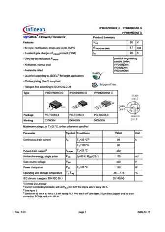
Type IPB037N06N3 G IPI040N06N3 G IPP040N06N3 G OptiMOS 3 Power-Transistor Product Summary Features V 60 V DS R 3.7 for sync. rectification, drives and dc/dc SMPS m DS(on),max (SMD) I 90 A Excellent gate charge x R product (FOM) D DS(on) previous engineering Very low on-resistance R DS(on) sample codes N-channel, normal level IPP04xN06N IPI04xN06N Ava... See More ⇒
9.6. Size:1003K infineon
ipb033n10n5lf.pdf
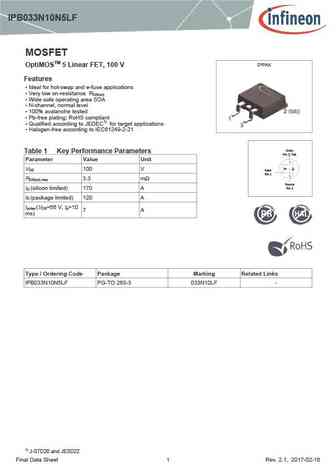
IPB033N10N5LF MOSFET D PAK OptiMOSTM 5 Linear FET, 100 V Features Ideal for hot-swap and e-fuse applications Very low on-resistance R DS(on) Wide safe operating area SOA N-channel, normal level 100% avalanche tested Pb-free plating; RoHS compliant Qualified according to JEDEC1) for target applications Halogen-free according to IEC61249-2-21 Drain ... See More ⇒
9.7. Size:508K infineon
ipb038n12n3-g ipi041n12n3-g ipp041n12n3-g.pdf
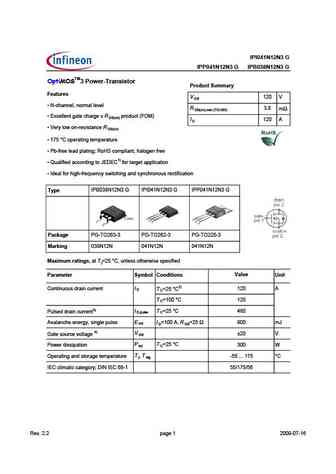
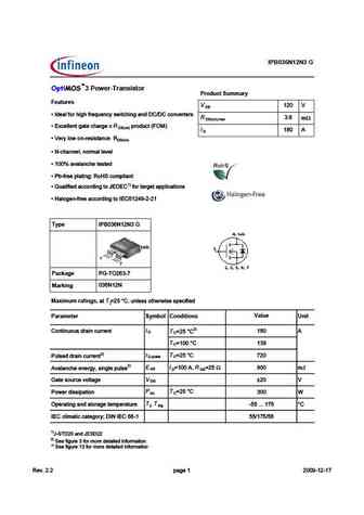
IPI041N12N3 G IPP041N12N3 G IPB038N12N3 G OptiMOSTM3 Power-Transistor Product Summary Features V 120 V DS N-channel, normal level R 3.8 m DS(on),max (TO-263) Excellent gate charge x R product (FOM) DS(on) I 120 A D Very low on-resistance R DS(on) 175 C operating temperature Pb-free lead plating; RoHS compliant, halogen free Qualified according to... See More ⇒
9.8. Size:534K infineon
ipb031ne7n3 ipb031ne7n3g.pdf
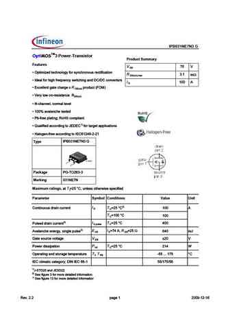
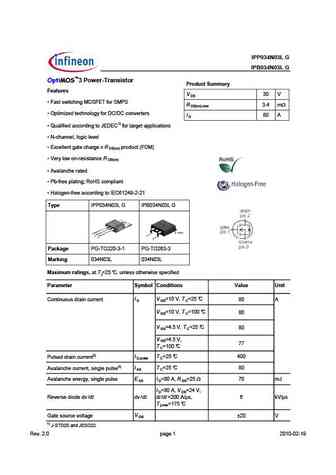
IPB031NE7N3 G TM 3 Power-Transistor Product Summary Features V 7 D Q ( @D9=9J54 D538>??EC B53D96931D9?> R 1 m D n) m x Q #4513I CG9D389>7 1>4 3?>F5BD5BC I 1 D Q H35... See More ⇒
9.9. Size:344K infineon
ipb039n04l-g ipp039n04l-g.pdf
Type IPP039N04L G IPB039N04L G OptiMOS 3 Power-Transistor Product Summary Features V 40 V DS Fast switching MOSFET for SMPS R 3.9 m DS(on),max Optimized technology for DC/DC converters I 80 A D Qualified according to JEDEC1) for target applications N-channel, logic level Excellent gate charge x R product (FOM) DS(on) Very low on-resistance R DS(on... See More ⇒
9.11. Size:279K infineon
ipb03n03lbg.pdf
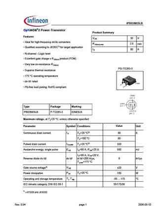
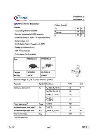
IPB03N03LB OptiMOS 2 Power-Transistor Product Summary Features V 30 V DS Ideal for high-frequency dc/dc converters R 2.8 m DS(on),max Qualified according to JEDEC1) for target application I 80 A D N-channel - Logic level Excellent gate charge x R product (FOM) DS(on) Very low on-resistance R DS(on) PG-TO220-3-1 PG-TO263-3 Superior thermal resistan... See More ⇒
9.12. Size:633K infineon
ipb036n12n3g.pdf
IPB036N12N3 G 3 Power-Transistor Product Summary Features V 1 D Q #4513I CG9D389>7 1>4 3?>F5BD5BC R m D n) m x Q H35... See More ⇒
9.14. Size:1124K infineon
ipb031n08n5.pdf
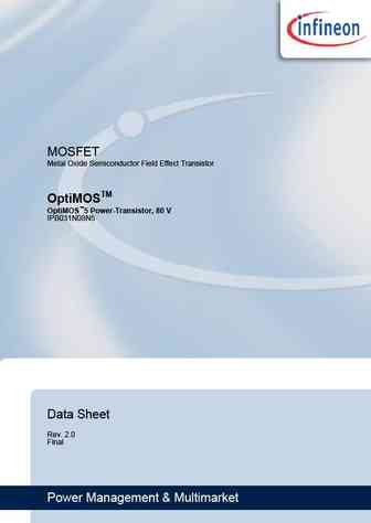
MOSFET Metal Oxide Semiconductor Field Effect Transistor OptiMOSTM OptiMOS 5 Power-Transistor, 80 V IPB031N08N5 Data Sheet Rev. 2.0 Final Power Management & Multimarket OptiMOS 5 Power-Transistor, 80 V IPB031N08N5 D PAK 1 Description Features Ideal for high frequency switching and sync. rec. Excellent gate charge x R product (FOM) DS(on) Very low on-resistance R... See More ⇒
9.15. Size:725K infineon
ipp034n03lg ipb034n03lg.pdf

Type IPP034N03L G IPB034N03L G 3 Power-Transistor Product Summary Features V 30 V DS Fast switching MOSFET for SMPS R 3.4 mW DS(on),max Optimized technology for DC/DC converters I 80 A D Qualified according to JEDEC1) for target applications N-channel, logic level Excellent gate charge x R product (FOM) DS(on) Very low on-resistance R DS(on) ... See More ⇒
9.16. Size:686K infineon
ipb039n04l.pdf
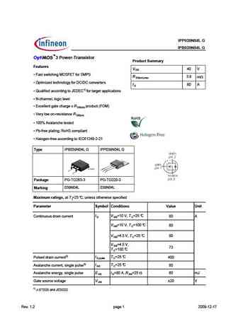
Type IPP039N04L G IPB039N04L G 3 Power-Transistor Product Summary Features V 40 V DS Fast switching MOSFET for SMPS R 3.9 mW DS(on),max Optimized technology for DC/DC converters I 80 A D Qualified according to JEDEC1) for target applications N-channel, logic level Excellent gate charge x R product (FOM) DS(on) Very low on-resistance R DS(on) ... See More ⇒
9.17. Size:1096K infineon
ipb032n10n5.pdf
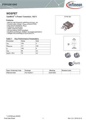
IPB032N10N5 MOSFET D -PAK 7pin OptiMOS 5 Power-Transistor, 100 V Features Ideal for high frequency switching and sync. rec. tab Excellent gate charge x R product (FOM) DS(on) Very low on-resistance R DS(on) N-channel, normal level 1 100% avalanche tested Pb-free plating; RoHS compliant 7 Qualified according to JEDEC1) for target applications H... See More ⇒
9.18. Size:873K infineon
ipi041n12n3g ipp041n12n3g ipb038n12n3g.pdf
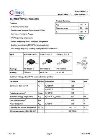
IPI041N12N3 G IPP041N12N3 G IPB038N12N3 G OptiMOSTM3 Power-Transistor Product Summary Features VDS 120 V N-channel, normal level RDS(on),max (TO-263) 3.8 mW Excellent gate charge x R product (FOM) DS(on) ID 120 A Very low on-resistance R DS(on) 175 C operating temperature Pb-free lead plating; RoHS compliant, halogen free Qualified according to JE... See More ⇒
9.19. Size:494K infineon
ipp037n08n3g ipi037n08n3g ipb035n08n3g.pdf
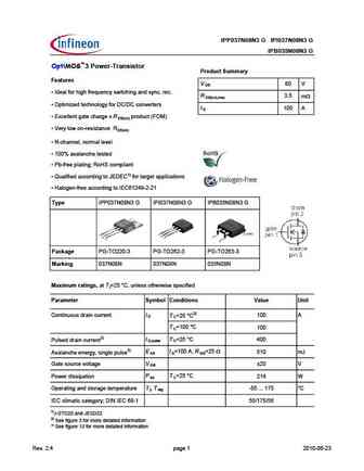
IPP037N08N3 G IPI037N08N3 G IPB035N08N3 G OptiMOS 3 Power-Transistor Product Summary Features V 80 V DS Ideal for high frequency switching and sync. rec. R 3.5 m DS(on),max Optimized technology for DC/DC converters I 100 A D Excellent gate charge x R product (FOM) DS(on) Very low on-resistance RDS(on) N-channel, normal level 100% avalanche tested ... See More ⇒
9.21. Size:723K infineon
ipb034n03l ipp034n03l.pdf
Type IPP034N03L G IPB034N03L G 3 Power-Transistor Product Summary Features V 30 V DS Fast switching MOSFET for SMPS R 3.4 mW DS(on),max Optimized technology for DC/DC converters I 80 A D Qualified according to JEDEC1) for target applications N-channel, logic level Excellent gate charge x R product (FOM) DS(on) Very low on-resistance R DS(on) ... See More ⇒
9.22. Size:258K inchange semiconductor
ipb033n10n5lf.pdf
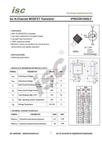
Isc N-Channel MOSFET Transistor IPB033N10N5LF FEATURES With To-263(D2PAK) package Low input capacitance and gate charge Low gate input resistance 100% avalanche tested Minimum Lot-to-Lot variations for robust device performance and reliable operation APPLICATIONS Switching applications ABSOLUTE MAXIMUM RATINGS(T =25 ) a SYMBOL PARAMETER VALUE UNIT V Drain-Source... See More ⇒
9.23. Size:258K inchange semiconductor
ipb038n12n3g.pdf

Isc N-Channel MOSFET Transistor IPB038N12N3G FEATURES With To-263(D2PAK) package Low input capacitance and gate charge Low gate input resistance 100% avalanche tested Minimum Lot-to-Lot variations for robust device performance and reliable operation APPLICATIONS Switching applications ABSOLUTE MAXIMUM RATINGS(T =25 ) a SYMBOL PARAMETER VALUE UNIT V Drain-Source ... See More ⇒
9.24. Size:228K inchange semiconductor
ipb035n08n3g.pdf
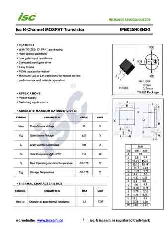
Isc N-Channel MOSFET Transistor IPB035N08N3G FEATURES With TO-263( D PAK ) packaging High speed switching Low gate input resistance Standard level gate drive Easy to use 100% avalanche tested Minimum Lot-to-Lot variations for robust device performance and reliable operation APPLICATIONS Power supply Switching applications ABSOLUTE MAXIMUM RATINGS(T =25 ) ... See More ⇒
9.25. Size:243K inchange semiconductor
ipb034n03l .pdf
isc N-Channel MOSFET Transistor IPB034N03L DESCRIPTION Drain Current I = 80A@ T =25 D C Drain Source Voltage V = 30V(Min) DSS 100% avalanche tested Minimum Lot-to-Lot variations for robust device performance and reliable operation APPLICATIONS . Designed for high current, high speed switching, switch mode power supplies. ABSOLUTE MAXIMUM RATINGS(T =25 ) C SY... See More ⇒
9.26. Size:258K inchange semiconductor
ipb037n06n3.pdf
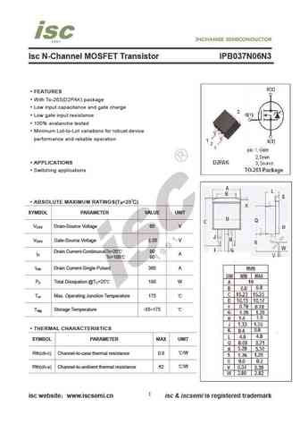
Isc N-Channel MOSFET Transistor IPB037N06N3 FEATURES With To-263(D2PAK) package Low input capacitance and gate charge Low gate input resistance 100% avalanche tested Minimum Lot-to-Lot variations for robust device performance and reliable operation APPLICATIONS Switching applications ABSOLUTE MAXIMUM RATINGS(T =25 ) a SYMBOL PARAMETER VALUE UNIT V Drain-Source V... See More ⇒
9.27. Size:258K inchange semiconductor
ipb034n06l3g.pdf

Isc N-Channel MOSFET Transistor IPB034N06L3G FEATURES With To-263(D2PAK) package Low input capacitance and gate charge Low gate input resistance 100% avalanche tested Minimum Lot-to-Lot variations for robust device performance and reliable operation APPLICATIONS Switching applications ABSOLUTE MAXIMUM RATINGS(T =25 ) a SYMBOL PARAMETER VALUE UNIT V Drain-Source ... See More ⇒
9.28. Size:258K inchange semiconductor
ipb031n08n5.pdf
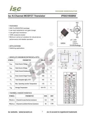
Isc N-Channel MOSFET Transistor IPB031N08N5 FEATURES With To-263(D2PAK) package Low input capacitance and gate charge Low gate input resistance 100% avalanche tested Minimum Lot-to-Lot variations for robust device performance and reliable operation APPLICATIONS Switching applications ABSOLUTE MAXIMUM RATINGS(T =25 ) a SYMBOL PARAMETER VALUE UNIT V Drain-Source V... See More ⇒
9.29. Size:219K inchange semiconductor
ipb039n04l.pdf
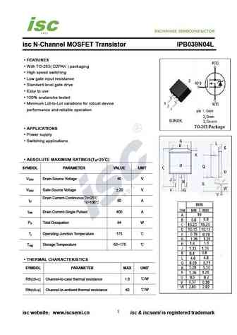
isc N-Channel MOSFET Transistor IPB039N04L FEATURES With TO-263( D2PAK ) packaging High speed switching Low gate input resistance Standard level gate drive Easy to use 100% avalanche tested Minimum Lot-to-Lot variations for robust device performance and reliable operation APPLICATIONS Power supply Switching applications ABSOLUTE MAXIMUM RATINGS(T =25 ) a ... See More ⇒
9.30. Size:243K inchange semiconductor
ipb034n03l.pdf
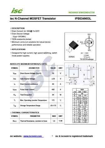
isc N-Channel MOSFET Transistor IPB034N03L DESCRIPTION Drain Current I = 80A@ T =25 D C Drain Source Voltage V = 30V(Min) DSS 100% avalanche tested Minimum Lot-to-Lot variations for robust device performance and reliable operation APPLICATIONS . Designed for high current, high speed switching, switch mode power supplies. ABSOLUTE MAXIMUM RATINGS(T =25 ) C SY... See More ⇒
9.31. Size:252K inchange semiconductor
ipb031ne7n3.pdf
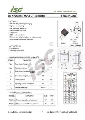
INCHANGE Semiconductor isc N-Channel MOSFET Transistor IPB031NE7N3 FEATURES With TO-263( D2PAK ) packaging High speed switching Low gate input resistance Standard level gate drive Easy to use 100% avalanche tested Minimum Lot-to-Lot variations for robust device performance and reliable operation APPLICATIONS Power supply Switching applications ABSOLUTE MAXI... See More ⇒
Detailed specifications: IPB021N06N3G, IPB022N04LG, IPB023N04NG, IPB023N06N3G, IPB025N08N3G, IPB025N10N3G, IPB027N10N3G, IPB029N06N3G, IRFP260N, IPB031NE7N3G, IPB034N03LG, IPB034N06L3G, IPB034N06N3G, IPB035N08N3G, IPB036N12N3G, IPB037N06N3G, IPB038N12N3G
Keywords - IPB030N08N3G MOSFET specs
IPB030N08N3G cross reference
IPB030N08N3G equivalent finder
IPB030N08N3G pdf lookup
IPB030N08N3G substitution
IPB030N08N3G replacement
Can't find your MOSFET?
Learn how to find a substitute transistor by analyzing voltage, current and package compatibility