SSM6J512NU Datasheet. Specs and Replacement
Type Designator: SSM6J512NU 📄📄
Type of Transistor: MOSFET
Type of Control Channel: P-Channel
Absolute Maximum Ratings
Pd ⓘ - Maximum Power Dissipation: 1.25 W
|Vds|ⓘ - Maximum Drain-Source Voltage: 12 V
|Vgs|ⓘ - Maximum Gate-Source Voltage: 10 V
|Id| ⓘ - Maximum Drain Current: 10 A
Tj ⓘ - Maximum Junction Temperature: 150 °C
Electrical Characteristics
Cossⓘ - Output Capacitance: 250 pF
RDSonⓘ - Maximum Drain-Source On-State Resistance: 0.0162 Ohm
Package: UDFN6B
📄📄 Copy
SSM6J512NU substitution
- MOSFET ⓘ Cross-Reference Search
SSM6J512NU datasheet
ssm6j512nu.pdf
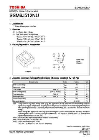
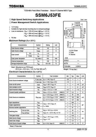
SSM6J512NU MOSFETs Silicon P-Channel MOS SSM6J512NU SSM6J512NU SSM6J512NU SSM6J512NU 1. Applications 1. Applications 1. Applications 1. Applications Power Management Switches 2. Features 2. Features 2. Features 2. Features (1) 1.8 V gate drive voltage. (2) Low drain-source on-resistance RDS(ON) = 24.0 m (typ.) (@VGS = -1.8 V) RDS(ON) = 18.3 m (typ.) (@VGS = -2.5 V... See More ⇒
ssm6j51tu.pdf
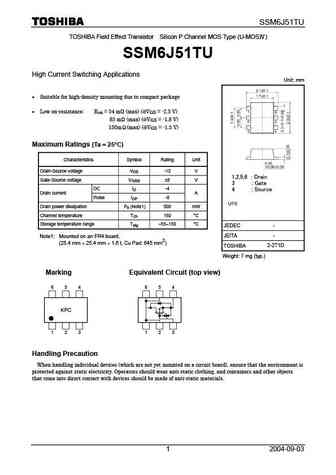
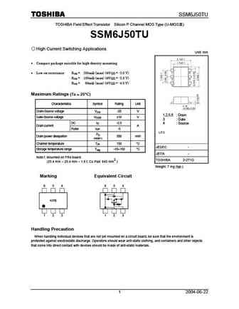
SSM6J51TU TOSHIBA Field Effect Transistor Silicon P Channel MOS Type (U-MOS ) SSM6J51TU High Current Switching Applications Unit mm Suitable for high-density mounting due to compact package Low on-resistance Ron = 54 m (max) (@VGS = -2.5 V) 85 m (max) (@VGS = -1.8 V) 150m (max) (@VGS = -1.5 V) Maximum Ratings (Ta = 25 C) Characteristics Symbol Rating Unit... See More ⇒
ssm6j511nu.pdf
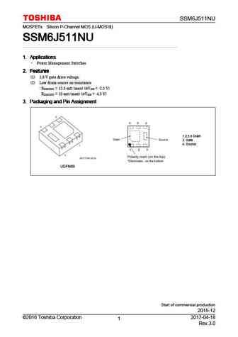
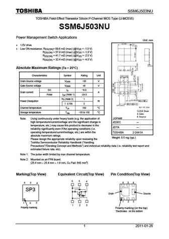
SSM6J511NU MOSFETs Silicon P-Channel MOS (U-MOS ) SSM6J511NU SSM6J511NU SSM6J511NU SSM6J511NU 1. Applications 1. Applications 1. Applications 1. Applications Power Management Switches 2. Features 2. Features 2. Features 2. Features (1) 1.8 V gate drive voltage. (2) Low drain-source on-resistance RDS(ON) = 13.5 m (max) (@VGS = -2.5 V) RDS(ON) = 10 m (max) (@VGS =... See More ⇒
ssm6j507nu.pdf
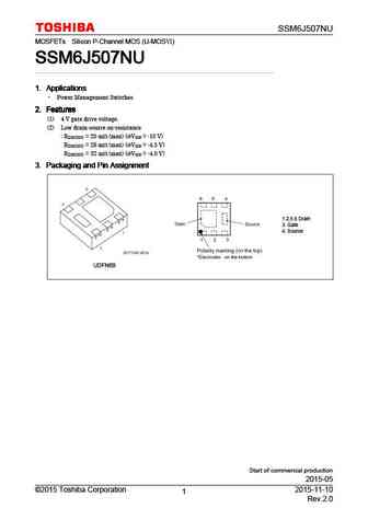
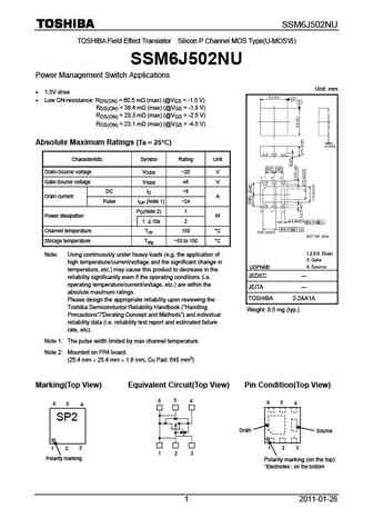
SSM6J507NU MOSFETs Silicon P-Channel MOS (U-MOS ) SSM6J507NU SSM6J507NU SSM6J507NU SSM6J507NU 1. Applications 1. Applications 1. Applications 1. Applications Power Management Switches 2. Features 2. Features 2. Features 2. Features (1) 4 V gate drive voltage. (2) Low drain-source on-resistance RDS(ON) = 20 m (max) (@VGS = -10 V) RDS(ON) = 28 m (max) (@VGS = -4.5... See More ⇒
Detailed specifications: SSM6680GM, SSM6923O, SSM6G18NU, SSM6H19NU, SSM6J216FE, SSM6J414TU, SSM6J505NU, SSM6J507NU, IRF3710, SSM6J771G, SSM6K217FE, SSM6K504NU, SSM6K781G, SSM6N55NU, SSM6N56FE, SSM6N57NU, SSM6N58NU
Keywords - SSM6J512NU MOSFET specs
SSM6J512NU cross reference
SSM6J512NU equivalent finder
SSM6J512NU pdf lookup
SSM6J512NU substitution
SSM6J512NU replacement
Can't find your MOSFET? Learn how to find a substitute transistor by analyzing voltage, current and package compatibility
History: 2SK3595-01MR | AFN8411
🌐 : EN ES РУ

LIST
Last Update
MOSFET: BCD70N07A | BCD90N03 | BCD80N06 | T50N06 | H50N06 | BCD12N65 | BCT12N65 | BCD4N65 | BCT4N65 | BCD7N65
Popular searches
j5027-r datasheet | transistor a1015 datasheet | bf199 transistor equivalent | bu801 | c8550 transistor datasheet | mj21194 transistor datasheet | kep40n26 | nte103a