BSC011N03LST. Аналоги и основные параметры
Наименование производителя: BSC011N03LST
Тип транзистора: MOSFET
Полярность: N
Предельные значения
Pd ⓘ
- Максимальная рассеиваемая мощность: 3 W
|Vds|ⓘ - Максимально допустимое напряжение сток-исток: 30 V
|Vgs|ⓘ - Максимально допустимое напряжение затвор-исток: 20 V
|Id| ⓘ - Максимально допустимый постоянный ток стока: 39 A
Tj ⓘ - Максимальная температура канала: 175 °C
Электрические характеристики
tr ⓘ -
Время нарастания: 8.8 ns
Cossⓘ - Выходная емкость: 1500 pf
RDSonⓘ - Сопротивление сток-исток открытого транзистора: 0.0011 Ohm
Тип корпуса: SUPERSO8
Аналог (замена) для BSC011N03LST
- подборⓘ MOSFET транзистора по параметрам
BSC011N03LST даташит
..1. Size:1260K infineon
bsc011n03lst.pdf 

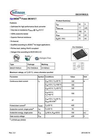
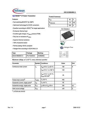
BSC011N03LST MOSFET TDSON-8 FL (enlarged source interconnection) OptiMOSTM Power-MOSFET, 30 V 8 7 6 Features 5 Optimized for high performance Buck converter 175 C rated 1 5 2 6 Very low on-resistance R @ V =4.5 V DS(on) GS 7 3 4 8 100% avalanche tested Superior thermal resistance 4 N-channel 3 Qualified according to JEDEC1) for target applicat
3.1. Size:698K infineon
bsc011n03lsi.pdf 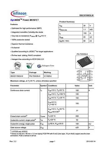
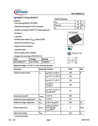
BSC011N03LSI OptiMOSTM Power-MOSFET Product Summary Features VDS 30 V Optimized for high performance SMPS RDS(on),max 1.1 mW Integrated monolithic Schottky-like diode ID 100 A Very low on-resistance R @ V =4.5 V DS(on) GS QOSS 45 nC 100% avalanche tested QG(0V..10V) 68 nC Superior thermal resistance N-channel Qualified according to JEDEC1) for
9.1. Size:976K infineon
bsc014n06nssc.pdf 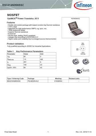
BSC014N06NSSC MOSFET PG-WSON-8-2 OptiMOSTM Power-Transistor, 60 V Features Double side cooled package-with lowest Junction-top thermal resistance tab 175 C rated Optimized for high performance SMPS, e.g. sync. rec. 5 6 100% avalanche tested 7 8 Superior thermal resistance 4 3 N-channel 2 1 Pb-free lead plating; RoHS compliant Halogen-free ac
9.2. Size:511K infineon
bsc014n06ns.pdf 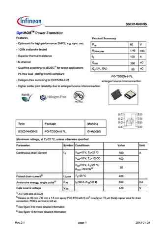
Type BSC014N06NS OptiMOSTM Power-Transistor Features Product Summary Optimized for high performance SMPS, e.g. sync. rec. VDS 60 V 100% avalanche tested RDS(on),max 1.45 mW Superior thermal resistance ID 100 A N-channel QOSS nC 100 Qualified according to JEDEC1) for target applications QG(0V..10V) nC 89 Pb-free lead plating; RoHS compliant PG-
9.5. Size:573K infineon
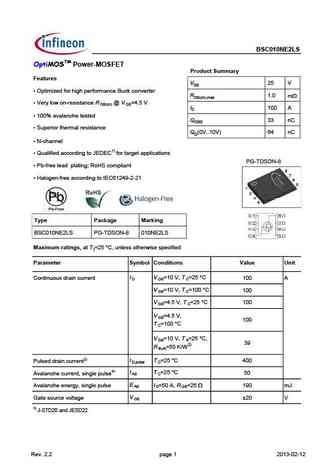
bsc010n04ls.pdf 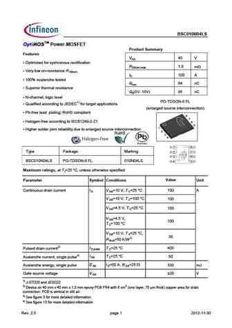
BSC010N04LS OptiMOSTM Power-MOSFET Product Summary Features VDS 40 V Optimized for sychronous rectification RDS(on),max 1.0 mW Very low on-resistance R DS(on) ID 100 A 100% avalanche tested Qoss 84 nC Superior thermal resistance Qg(0V..10V) 95 nC N-channel, logic level PG-TDSON-8 FL Qualified according to JEDEC1) for target applications (enlarg
9.6. Size:641K infineon
bsc014n04ls.pdf 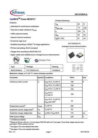
BSC014N04LS OptiMOSTM Power-MOSFET Product Summary Features VDS 40 V Optimized for synchronous rectification RDS(on),max 1.4 mW Very low on-state resistance R DS(on) ID 100 A 100% avalanche tested Qoss 54 nC Superior thermal resistance Qg(0V..10V) 61 nC N-channel, logic level PG-TDSON-8 FL Qualified according to JEDEC1) for target applications (
9.7. Size:1279K infineon
bsc010n04lst.pdf 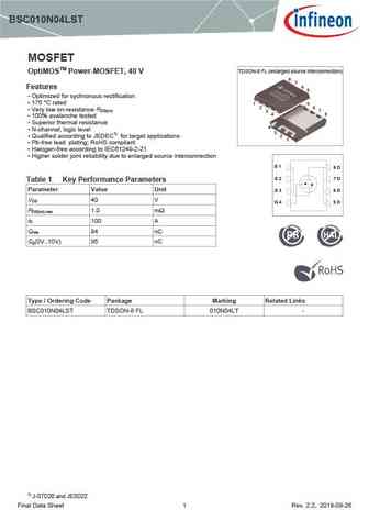
BSC010N04LST MOSFET TDSON-8 FL (enlarged source interconnection) OptiMOSTM Power-MOSFET, 40 V 8 7 6 Features 5 Optimized for sychronous rectification 175 C rated 1 5 2 6 Very low on-resistance R DS(on) 7 3 4 8 100% avalanche tested Superior thermal resistance 4 N-channel, logic level 3 Qualified according to JEDEC1) for target applications 2
9.8. Size:526K infineon
bsc019n04ls.pdf 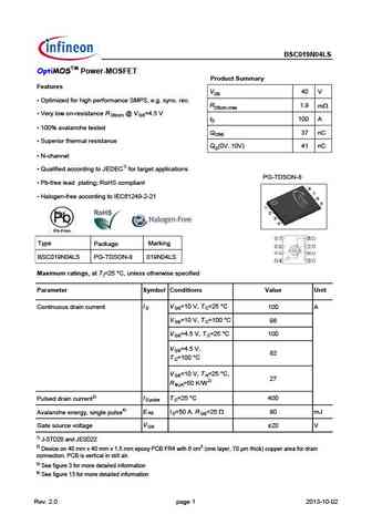
BSC019N04LS OptiMOSTM Power-MOSFET Product Summary Features VDS 40 V Optimized for high performance SMPS, e.g. sync. rec. RDS(on),max 1.9 mW Very low on-resistance R @ V =4.5 V DS(on) GS ID 100 A 100% avalanche tested QOSS 37 nC Superior thermal resistance QG(0V..10V) 41 nC N-channel Qualified according to JEDEC1) for target applications PG-TDSON-
9.9. Size:598K infineon
bsc014n04lsi.pdf 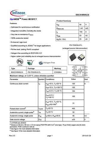
BSC014N04LSI OptiMOSTM Power-MOSFET Product Summary Features VDS 40 V Optimized for synchronous rectification RDS(on),max 1.45 mW Integrated monolithic Schottky-like diode A ID 100 Very low on-resistance R DS(on) QOSS 53 nC 100% avalanche tested 55 nC QG(0V..10V) N-channel, logic level PG-TDSON-8 FL Qualified according to JEDEC1) for target a
9.10. Size:1476K infineon
bsc010n04ls6.pdf 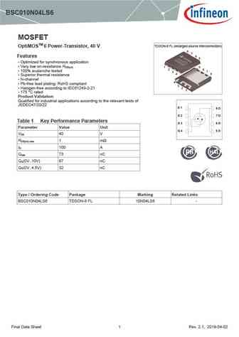
BSC010N04LS6 MOSFET TDSON-8 FL (enlarged source interconnection) OptiMOSTM 6 Power-Transistor, 40 V 8 7 6 Features 5 Optimized for synchronous application Very low on-resistance R DS(on) 1 5 2 6 100% avalanche tested 7 3 4 8 Superior thermal resistance N-channel 4 Pb-free lead plating; RoHS compliant 3 Halogen-free according to IEC61249-2-21 2
9.11. Size:598K infineon
bsc010n04lsi.pdf 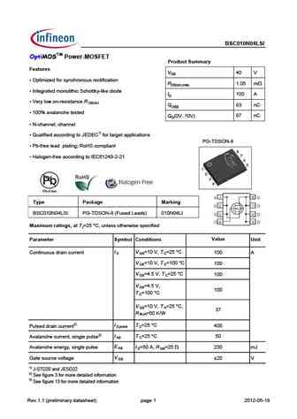
BSC010N04LSI OptiMOSTM Power-MOSFET Product Summary Features VDS 40 V Optimized for synchronous rectification RDS(on),max 1.05 mW Integrated monolithic Schottky-like diode A ID 100 Very low on-resistance R DS(on) QOSS 83 nC 100% avalanche tested 87 nC QG(0V..10V) N-channel, channel Qualified according to JEDEC1) for target applications PG-TDSO
9.12. Size:363K infineon
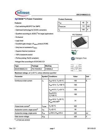
bsc018n04lsg.pdf 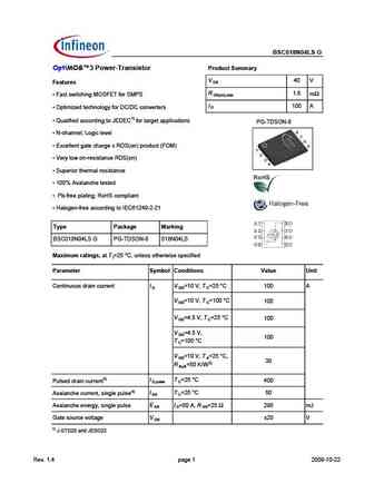
BSC018N04LS G OptiMOS 3 Power-Transistor Product Summary V 40 V Features DS R 1.8 m Fast switching MOSFET for SMPS DS(on),max I 100 A Optimized technology for DC/DC converters D Qualified according to JEDEC1) for target applications PG-TDSON-8 N-channel; Logic level Excellent gate charge x RDS(on) product (FOM) Very low on-resistance RDS(on) Superi
9.14. Size:836K infineon
bsc012n06ns.pdf 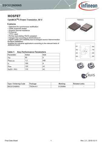
BSC012N06NS MOSFET TSON-8-3 OptiMOSTM5 Power-Transistor, 60 V 8 7 5 6 6 Features 7 5 8 Optimized for synchronous rectification Pin 1 100% avalanche tested 2 4 3 3 Superior thermal resistance 4 2 1 N-channel 175 C rated Pb-free lead plating; RoHS compliant Halogen-free according to IEC61249-2-21 Higher solder joint reliability due to enla
9.15. Size:679K infineon
bsc016n03ls .pdf 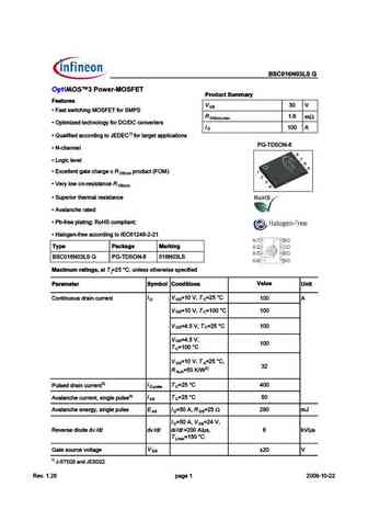
& " & E $;B1= !#& ' $=;0@/? &@99-=D Features D Q 2CD CG D49 ?8 ') - . 7@B -'*- 1 m D n) m x Q ) AD > J65 D649?@=@8I 7@B 4@?F6BD6BC 1 D 1) Q + E2= 7 65 244@B5 ?8 D@ $ 7@B D2B86D 2AA= 42D @?C G D ON Q ( 492??6= Q &@8 4 =6F6= Q H46==6?D 82D6 492B86 H AB@5E4D ) ' D n) Q /6BI =@G @? B6C CD2?46 D n) Q -EA6B @B D96B>2= B6C CD2?46 Q F2=2?496 B2D65 Q *3 7B66 A=2
9.17. Size:1264K infineon
bsc016n06nst.pdf 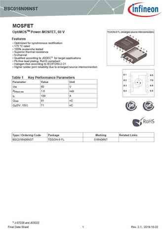
BSC016N06NST MOSFET TDSON-8 FL (enlarged source interconnection) OptiMOSTM Power-MOSFET, 60 V 8 7 6 Features 5 Optimized for synchronous rectification 175 C rated 1 5 2 6 100% avalanche tested 7 3 4 8 Superior thermal resistance N-channel 4 Qualified according to JEDEC1) for target applications 3 Pb-free lead plating; RoHS compliant 2 1
9.18. Size:542K infineon
bsc016n03msg.pdf 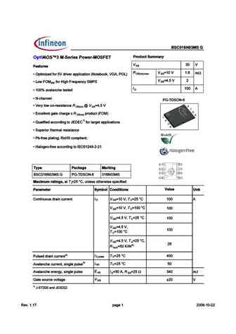
% ! % # %?88, G D ON S 07DK >AI A@ D7E;EF3@57 0 D n) G S J57>>7@F 93F7 5 3D97 J BDA6G5F !* ( D n) 1) S , G3>;8;76 355AD6;@9 FA % 8AD F3D97F 3BB>;53F;A@E S .GB7D;AD
9.19. Size:1788K infineon
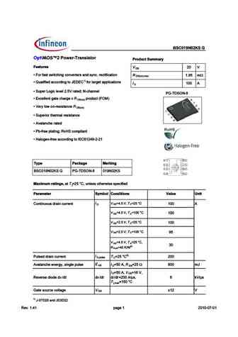
bsc010ne2lsi.pdf 
MOSFET Metal Oxide Semiconductor Field Effect Transistor OptiMOSTM OptiMOSTM Power-MOSFET, 25 V BSC010NE2LSI Data Sheet Rev. 2.3 Final Power Management & Multimarket OptiMOSTM Power-MOSFET, 25 V BSC010NE2LSI SuperSO8 1 Description 5 8 6 7 Features 7 6 8 5 Optimized for high performance Buck converter Monolithic integrated Schottky like diode Very low on-resi
9.20. Size:699K infineon
bsc014ne2lsi.pdf 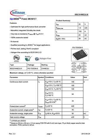
BSC014NE2LSI OptiMOSTM Power-MOSFET Product Summary Features VDS 25 V Optimized for high performance Buck converter RDS(on),max 1.4 mW Monolithic integrated Schottky like diode A ID 100 Very low on-resistance R @ V =4.5 V DS(on) GS QOSS 25 nC 100% avalanche tested 39 nC QG(0V..10V) N-channel Qualified according to JEDEC1) for target applicatio
9.21. Size:700K infineon
bsc014n03ls .pdf 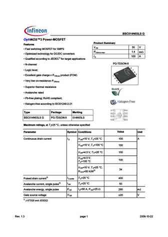
& " & E $;B1= !#& ' $=;0@/? &@99-=y Features D Q 2CD CG D49 ?8 ') - . 7@B -'*- 1 4 m D n) m x Q ) AD > J65 D649?@=@8I 7@B 4@?F6BD6BC 1 D 1) Q + E2= 7 65 244@B5 ?8 D@ $ 7@B D2B86D 2AA= 42D @?C G D ON Q ( 492??6= Q &@8 4 =6F6= Q H46==6?D 82D6 492B86 H AB@5E4D ) ' D n) Q /6BI =@G @? B6C CD2?46 D n) Q -EA6B @B D96B>2= B6C CD2?46 Q F2=2?496 B2D65 Q *3 7B66 A=2
9.23. Size:566K infineon
bsc016n06ns.pdf 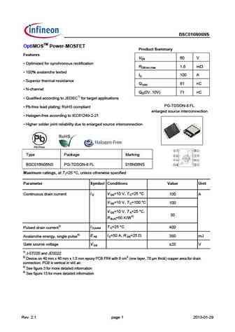
BSC016N06NS OptiMOSTM Power-MOSFET Product Summary Features VDS 60 V Optimized for synchronous rectification RDS(on),max 1.6 mW 100% avalanche tested ID 100 A Superior thermal resistance QOSS 81 nC N-channel QG(0V..10V) 71 nC Qualified according to JEDEC1) for target applications PG-TDSON-8 FL Pb-free lead plating; RoHS compliant enlarged source
9.24. Size:1615K infineon
bsc018ne2ls.pdf 
n-Channel Power MOSFET OptiMOS BSC018NE2LS Data Sheet 2.1, 2011-09-20 Final Industrial & Multimarket OptiMOS Power-MOSFET BSC018NE2LS 1 Description OptiMOS 25V products are class leading power MOSFETs for highest power density and energy efficient solutions. Ultra low gate- and output charges together with lowest on state resistance in small footprint packages make OptiMO
9.25. Size:379K infineon
bsc017n04nsg.pdf 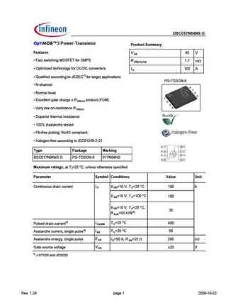
BSC017N04NS G OptiMOS 3 Power-Transistor Product Summary Features V 40 V DS Fast switching MOSFET for SMPS R 1.7 m DS(on),max Optimized technology for DC/DC converters I 100 A D Qualified according to JEDEC1) for target applications PG-TDSON-8 N-channel Normal level Excellent gate charge x R product (FOM) DS(on) Very low on-resistance R DS(on
9.28. Size:463K infineon
bsc014n03ls.pdf 
BSC014N03LS G OptiMOS 3 Power-MOSFET Product Summary Features V 30 V DS Fast switching MOSFET for SMPS R 1.4 m DS(on),max Optimized technology for DC/DC converters I 100 A D Qualified according to JEDEC1) for target applications PG-TDSON-8 N-channel Logic level; Excellent gate charge x R product (FOM) DS(on) Very low on-resistance R DS(on)
9.29. Size:466K infineon
bsc014n03lsg.pdf 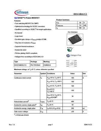
BSC014N03LS G OptiMOS 3 Power-MOSFET Product Summary Features V 30 V DS Fast switching MOSFET for SMPS R 1.4 m DS(on),max Optimized technology for DC/DC converters I 100 A D Qualified according to JEDEC1) for target applications PG-TDSON-8 N-channel Logic level; Excellent gate charge x R product (FOM) DS(on) Very low on-resistance R DS(on)
9.30. Size:540K infineon
bsc014n03msg.pdf 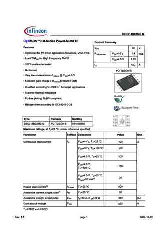
% ! % D %0 G D ON S 07DK >AI A@ D7E;EF3@57 0 D n) G S J57>>7@F 93F7 5 3D97 J BDA6G5F !* ( D n) 1) S , G3>;8;76 355AD6;@9 FA % 8AD F3D97F 3BB>;53F;A@E S .GB
9.31. Size:637K infineon
bsc018ne2lsi.pdf 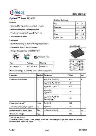
BSC018NE2LSI OptiMOSTM Power-MOSFET Product Summary Features VDS 25 V Optimized for high performance Buck converter RDS(on),max 1.8 mW Monolithic integrated Schottky like diode A ID 100 Very low on-resistance R @ V =4.5 V DS(on) GS QOSS 23 nC 100% avalanche tested 36 nC QG(0V..10V) N-channel Qualified according to JEDEC1) for target applicatio
9.32. Size:194K infineon
bsc016n03ms.pdf 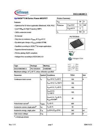
BSC016N03MS G Product Summary OptiMOS 3 M-Series Power-MOSFET V 30 V DS Features R V =10 V 1.6 m DS(on),max GS Optimized for 5V driver application (Notebook, VGA, POL) V =4.5 V 2 GS Low FOMSW for High Frequency SMPS I 100 A D 100% avalanche tested N-channel PG-TDSON-8 Very low on-resistance R @ V =4.5 V DS(on) GS Excellent gate charge x R product
9.33. Size:194K infineon
bsc014n03ms.pdf 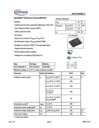
BSC014N03MS G OptiMOS 3 M-Series Power-MOSFET Product Summary Features V 30 V DS Optimized for 5V driver application (Notebook, VGA, POL) R V =10 V 1.4 m DS(on),max GS Low FOMSW for High Frequency SMPS V =4.5 V 1.75 GS 100% avalanche tested I 100 A D N-channel PG-TDSON-8 Very low on-resistance R @ V =4.5 V DS(on) GS Excellent gate charge x R prod
9.34. Size:1566K infineon
bsc015ne2ls5i.pdf 
MOSFET Metal Oxide Semiconductor Field Effect Transistor OptiMOSTM OptiMOSTM5 Power-MOSFET, 25 V BSC015NE2LS5I Data Sheet Rev. 2.0 Final Power Management & Multimarket OptiMOSTM5 Power-MOSFET, 25 V BSC015NE2LS5I SuperSO8 1 Description 5 8 6 7 Features 7 6 8 5 Optimized for high performance buck converters Monolithic integrated Schottky-like diode Very low on
9.35. Size:3484K cn vbsemi
bsc019n04ns.pdf 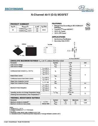
BSC019N04NS www.VBsemi.tw N-Channel 40-V (D-S) MOSFET FEATURES PRODUCT SUMMARY Halogen-free According to IEC 61249-2-21 VDS (V) RDS(on) ( ) ID (A)a Qg (Typ.) Definition 0.0025 at VGS = 10 V 120 TrenchFET Power MOSFET 40 38 nC 0.0028 at VGS = 6.5 V 105 100 % Rg Tested 100 % UIS Tested APPLICATIONS Synchronous Rectification Secondary Side DC/DC D
Другие MOSFET... AIMW120R045M1
, AUIRLS8409-7P
, BF2040
, BF2040R
, BF2040W
, BSC007N04LS6
, BSC010N04LS6
, BSC010N04LST
, 20N50
, BSC014N06NSSC
, BSC015NE2LS5I
, BSC016N06NST
, BSC021N08NS5
, BSC022N04LS6
, BSC027N06LS5
, BSC034N10LS5
, BSC0402NS
.
History: BSC0501NSI
| BSC032NE2LS
| IRC730PBF