J111 Specs and Replacement
Type Designator: J111
Type of Transistor: JFET
Type of Control Channel: N -Channel
Absolute Maximum Ratings
Pd ⓘ - Maximum Power Dissipation: 0.4 W
|Vds|ⓘ - Maximum Drain-Source Voltage: 35 V
|Id| ⓘ - Maximum Drain Current: 0.05 A
Tj ⓘ - Maximum Junction Temperature: 150 °C
Electrical Characteristics
Cossⓘ - Output Capacitance: 3 pF
Rds ⓘ - Maximum Drain-Source On-State Resistance: 30 Ohm
Package: TO92
J111 substitution
J111 datasheet
j111 j112 j113 cnv.pdf
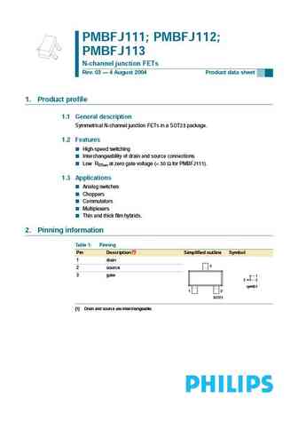
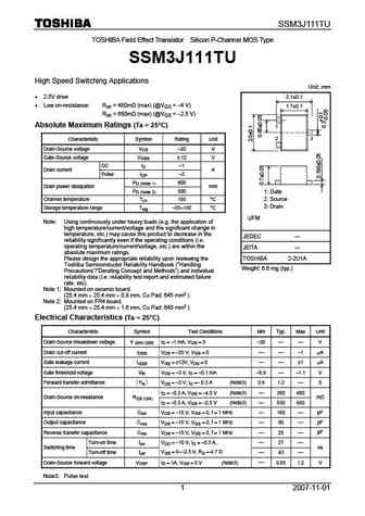
DISCRETE SEMICONDUCTORS DATA SHEET J111; J112; J113 N-channel silicon field-effect transistors July 1993 Product specification File under Discrete Semiconductors, SC07 Philips Semiconductors Product specification N-channel silicon field-effect transistors J111; J112; J113 DESCRIPTION Symmetrical silicon n-channel junction FETs in plastic TO-92 envelopes. They are intended for app... See More ⇒
j111 j112 j113 mmbfj111 mmbfj112 mmbfj113.pdf
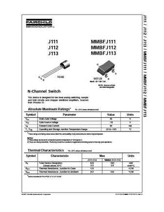
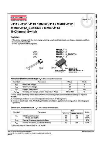
J111 MMBFJ111 J112 MMBFJ112 J113 MMBFJ113 G S G TO-92 S SOT-23 D D Mark 6P / 6R / 6S NOTE Source & Drain are interchangeable N-Channel Switch This device is designed for low level analog switching, sample and hold circuits and chopper stabilized amplifiers. Sourced from Process 51. Absolute Maximum Ratings* TA = 25 C unless otherwise noted Symbol Parameter Value Units VDG D... See More ⇒
j111 j112 j113 sst111 sst112 sst113.pdf
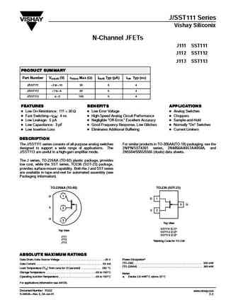
J/SST111 Series Vishay Siliconix N-Channel JFETs J111 SST111 J112 SST112 J113 SST113 PRODUCT SUMMARY Part Number VGS(off) (V) rDS(on) Max (W) ID(off) Typ (pA) tON Typ (ns) J/SST111 3 to 10 30 5 4 J/SST112 1 to 5 50 5 4 J/SST113 v 3 100 5 4 FEATURES BENEFITS APPLICATIONS D Low On-Resistance 111 ... See More ⇒
j111 j112.pdf
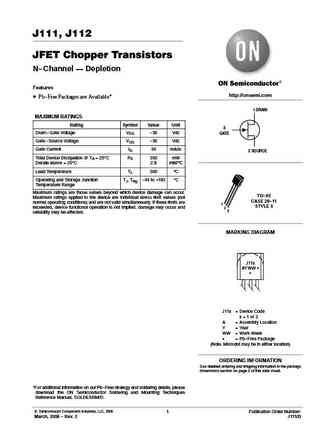
J111, J112 JFET Chopper Transistors N-Channel Depletion Features http //onsemi.com Pb-Free Packages are Available* 1 DRAIN MAXIMUM RATINGS Rating Symbol Value Unit 3 Drain-Gate Voltage VDG -35 Vdc GATE Gate -Source Voltage VGS -35 Vdc Gate Current IG 50 mAdc 2 SOURCE Total Device Dissipation @ TA = 25 C PD 350 mW Derate above = 25 C 2.8 mW/ C Lead Temperature TL 300 ... See More ⇒
Detailed specifications: IXTZ35N25MB , IXTZ42N20MA , IXTZ42N20MB , IXTZ67N10MA , IXTZ67N10MB , J108 , J109 , J110 , IRFP260N , J112 , J113 , J211 , J212 , JANSR2N7272 , JANSR2N7275 , JANSR2N7278 , JANSR2N7292 .
Keywords - J111 MOSFET specs
J111 cross reference
J111 equivalent finder
J111 pdf lookup
J111 substitution
J111 replacement
Step-by-step guide to finding a MOSFET replacement. Cross-reference parts and ensure compatibility for your repair or project.


